| No. | Inverter tutorial series |
|---|---|
| 1 | Basics of Inverters with Topology |
| 2 | Major Components of Inverters |
| 3 | Pure Sine Wave Inverter Design with Code |
| 4 | Modified Sine Wave Inverter Design with Code |
Hello friends, I hope you are doing well. In the previous tutorial, we studied the basic inverter topologies. We will now examine the components that turn a topology into a working power converter.
An inverter is a system rather than a single H-bridge. The controller creates switching commands, gate drivers translate those commands into high-current gate pulses, power semiconductors process energy, capacitors and magnetics store and filter it, sensors close the feedback loop, and protection circuits stop unsafe operation. The thermal design, PCB layout and enclosure are also functional parts of the converter.
We will follow the energy path from the DC input to the AC output and add the control and protection blocks around it. The exact parts depend on voltage, power, isolation, switching frequency, waveform and applicable safety standards.
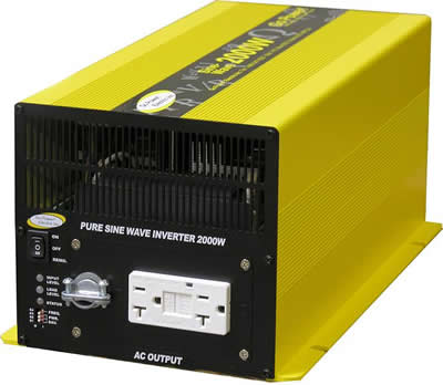
Functional Blocks of an Inverter
| Block | Main components | Purpose |
|---|---|---|
| DC input | Fuse, disconnect, reverse-polarity device, EMI filter | Connects and protects the energy source |
| DC link | Electrolytic and film capacitors, precharge circuit | Supports pulsed current and stabilizes bus voltage |
| Power stage | MOSFETs, IGBTs, SiC or GaN switches | Applies controlled voltage states to the load or transformer |
| Gate drive | Driver ICs, isolated supplies, gate resistors | Charges gates quickly and enforces safe switching |
| Magnetics and filter | Transformer, inductors, capacitors | Changes voltage, isolates and removes switching ripple |
| Control | MCU, DSC, DSP, FPGA or analog controller | Generates PWM and regulates voltage or current |
| Sensing | Shunts, current transformers, Hall sensors, dividers | Measures the electrical and thermal state |
| Protection | Comparators, TVS devices, snubbers, thermal sensors | Limits fault energy and electrical stress |
| Thermal system | Copper area, heat sinks, interface pads and fans | Keeps junction and winding temperatures within ratings |
1. DC Source, Fuse and Input Connections
The DC source determines the current level seen by the input stage. A 1 kW inverter operating from 12 V at 90% efficiency requires approximately:
Iin = Pout / (efficiency × Vdc)
Iin = 1000 W / (0.90 × 12 V) = 92.6 A
This current is before surge allowance and before battery voltage falls under load. The fuse, disconnect, cable, connector, PCB copper and current sensor must carry the worst continuous and transient current. Place the primary fuse close to the battery or source so an upstream cable fault is also protected.
A soft-start or precharge circuit limits the current that charges an empty DC-link capacitor. Without it, connecting a battery to a large capacitor can produce a damaging spark and stress connectors, fuses and capacitor terminals.
2. DC-Link Capacitors
The DC link supplies rapid switching current locally and reduces the impedance between bridge legs. It normally combines bulk electrolytic capacitors for low-frequency energy storage with low-inductance film or ceramic capacitors close to the switching loop.
Capacitor energy is:
E = 1/2 × C × V²
A 470 µF capacitor charged to 325 V stores:
E = 0.5 × 470 × 10^-6 F × (325 V)² = 24.8 J
That is hazardous energy. A discharge resistor and a verified safe-discharge time are necessary, but a resistor must not be assumed to work without measurement. Capacitor voltage rating, ripple-current rating, ESR, lifetime at temperature and fault current are as important as capacitance.
3. Controller
A microcontroller, digital signal controller, DSP, FPGA or analog control IC generates the switching pattern and supervises the system. It may perform:
- Sinusoidal or modified-wave PWM generation.
- Complementary outputs with hardware dead time.
- Output-voltage and current feedback control.
- Battery undervoltage and bus overvoltage supervision.
- Soft start, shutdown sequencing and fault logging.
- Temperature monitoring and fan control.
- User display, communication and diagnostics.
PWM resolution matters because the controller must represent the sine reference at the chosen carrier frequency. If a timer clock is 100 MHz and PWM is 20 kHz, an ideal edge-aligned timer has:
Counts per PWM period = 100,000,000 / 20,000 = 5000
The controller also needs deterministic fault response. A software loop running every millisecond is too slow to protect a bridge from a shoot-through event that can become destructive within microseconds. Hardware comparators, PWM trip inputs and gate-driver shutdown pins handle fast faults, while firmware manages recovery and reporting.
4. Bipolar Junction Transistors
A bipolar junction transistor is a current-controlled semiconductor device with base, collector and emitter terminals. NPN and PNP devices are useful in signal conditioning, gate-drive stages, relay control, current sources and some lower-frequency switching circuits.
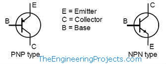
For a saturated BJT switch, the designer supplies enough base current to keep collector-emitter voltage low at the intended collector current. A simplified forced-gain calculation is:
Ib = Ic / forced beta
If a transistor must switch 200 mA and a conservative forced beta of 10 is selected, the base current is 20 mA. That drive requirement becomes inconvenient at high bridge power, which is one reason MOSFETs and IGBTs dominate modern inverter power stages.
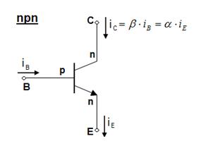
NPN Transistor
An NPN transistor used as a low-side switch has its emitter near ground and its load connected between the positive supply and collector. Raising the base above the emitter through a calculated resistor turns it on.
PNP Transistor
A PNP transistor can serve as a high-side switch at modest voltage. It turns on when its base is pulled below its emitter by the required base-emitter voltage. At inverter power and switching speed, a purpose-built gate driver with MOSFETs or IGBTs is usually more suitable.
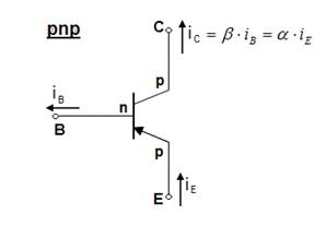
The transistor symbol's emitter arrow distinguishes NPN and PNP devices. Device polarity alone does not determine suitability; voltage, current, safe operating area, switching time, gain, storage time and thermal resistance must all meet the circuit requirements.
5. H-Bridge Power Stage
A single-phase H-bridge contains four controlled switches in two legs. One diagonal pair applies positive DC-link voltage to the load, and the opposite diagonal applies negative voltage. PWM zero states allow average voltage to follow a sine reference.
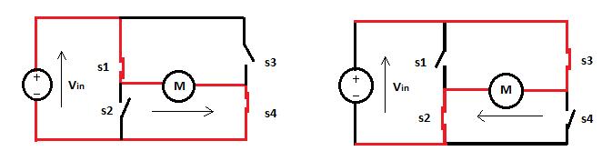
| Command | Switch pair | Ideal output |
|---|---|---|
| Positive state | S1 and S4 | +Vdc |
| Negative state | S2 and S3 | -Vdc |
| Forbidden state in left leg | S1 and S2 together | DC-link short circuit |
| Forbidden state in right leg | S3 and S4 together | DC-link short circuit |
The forbidden condition is shoot-through. Dead time gives one switch time to stop conducting before its complement turns on. Dead time must include driver propagation mismatch, switch turn-off delay, gate discharge and worst-case temperature behavior. It should then be confirmed with suitable differential voltage and current measurements.
6. Power MOSFETs
A power MOSFET is a voltage-driven device, but its gate is capacitive and requires current during switching. N-channel enhancement MOSFETs are most common in inverter bridges because they generally offer lower resistance than comparable P-channel devices.
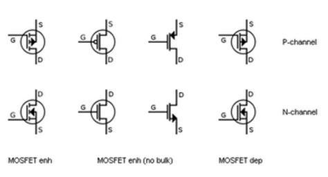
Important datasheet parameters include:
- Drain-source voltage rating with transient margin.
- On-resistance at the actual gate voltage and junction temperature.
- Total gate charge and Miller charge.
- Output capacitance and stored energy.
- Body-diode reverse recovery.
- Safe operating area and avalanche rating.
- Junction-to-case and junction-to-ambient thermal resistance.
First-order conduction loss for one MOSFET is:
Pconduction = Irms² × RDS(on) × conduction fraction
If a device carries 20 A RMS for half the time and its hot on-resistance is 8 mΩ:
Pconduction = (20 A)² × 0.008 ohm × 0.5 = 1.6 W
A rough hard-switching estimate is:
Pswitching ≈ 1/2 × VDS × ID × (tr + tf) × fs
This estimate omits capacitance, diode recovery and nonlinear transitions, but it shows why voltage, current, edge time and switching frequency all affect loss.
7. IGBTs, SiC MOSFETs and GaN Devices
IGBTs combine an insulated gate with bipolar conduction and remain useful at high voltage and moderate switching frequency. Their conduction loss is often represented by a collector-emitter saturation voltage rather than a simple low resistance.
Silicon-carbide MOSFETs support high bus voltage, fast switching and high junction temperature with low switching loss, while gallium-nitride devices offer very fast transitions and low charge in suitable voltage classes. Faster devices demand tighter layout, controlled gate impedance and careful electromagnetic-interference design. The newest technology is not automatically the best choice when cost, fault robustness and layout capability are considered.
Texas Instruments surveys conventional H-bridge and advanced inverter stages in its power-topology application report. Use the chosen semiconductor manufacturer's switching and gate-drive recommendations for the actual device.
8. Gate Drivers
The controller pin should not normally drive a power-switch gate directly. A gate-driver IC sources and sinks the pulse current needed to charge and discharge the gate quickly. High-side N-channel devices also need a gate voltage above their moving source node, produced by a bootstrap circuit or isolated supply.
Approximate gate-drive power for identical switches is:
Pgate = N × Qg × Vgate × fs
For four MOSFETs with 80 nC total gate charge, 12 V drive and 20 kHz switching:
Pgate = 4 × 80 nC × 12 V × 20 kHz = 0.0768 W
The average is modest, but the driver must supply much larger peak current during each edge. Gate resistors control ringing and switching speed. A gate-source pull-down holds the device off when the driver is unpowered, and a Miller clamp or negative turn-off bias may be useful in high-dv/dt systems.
Driver features may include undervoltage lockout, desaturation detection, short-circuit protection, active Miller clamping, isolated signal transfer and reinforced isolation. Choose isolation ratings from the actual bus voltage, transient environment and safety standard.
9. Transformer
A transformer transfers AC energy through changing magnetic flux. It can change voltage and provide galvanic isolation. A line-frequency inverter uses a large 50 Hz or 60 Hz transformer, while a two-stage inverter may use a smaller high-frequency transformer in its DC-DC stage.
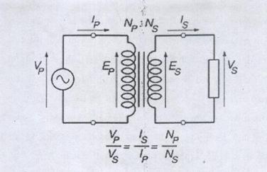
For an ideal transformer:
Vs / Vp = Ns / Np
Is / Ip = Np / Ns
Vp × Ip = Vs × Is
Here Vp and Ip are primary voltage and current, Vs and Is are secondary voltage and current, and Np and Ns are turns. A real transformer has copper loss, core loss, leakage inductance, magnetizing current, winding capacitance and temperature rise.
The turns ratio alone does not complete the design. Core material, frequency, maximum flux density, winding window, insulation system, creepage, clearance and cooling determine whether the transformer can carry the required power safely. Any DC imbalance in a low-frequency push-pull waveform can walk the core toward saturation.
10. Inductors and Output Filters
A sine-wave inverter commonly uses an LC low-pass filter. The inductor is placed in series with the output current and the capacitor is placed across the load side, although practical filters may use additional damping or multiple stages.
The ideal undamped resonant frequency is:
fc = 1 / (2π√(LC))
If L = 2 mH and C = 2.2 µF:
fc = 1 / (2π√(0.002 × 2.2 × 10^-6)) ≈ 2.40 kHz
That frequency is above a 50 Hz fundamental and below a typical 20 kHz carrier, but it is only a starting point. The filter must be designed with the load and feedback loop. Check inductor saturation, copper loss, core loss, capacitor ripple current, voltage rating, dielectric type and resonance damping.
An LC filter does dissipate real power because practical inductors have winding and core losses and capacitors have ESR and dielectric loss. It is usually more efficient than an RC power filter because it does not intentionally burn the unwanted voltage in a large series resistor.
11. Voltage, Current and Temperature Sensors
Feedback makes regulation and protection possible. A resistor divider can scale a DC voltage, but high-voltage sensing must meet power, spacing and transient requirements. Isolated amplifiers or transformers may be required across an isolation barrier.
Current can be measured with:
- A shunt resistor and differential or isolated amplifier.
- A current transformer for AC or pulsed current.
- A Hall-effect sensor for isolated DC and AC measurement.
- A Rogowski coil for rapidly changing current in specialized systems.
Shunt power is:
Pshunt = Irms² × Rshunt
A 2 mΩ shunt carrying 50 A dissipates 5 W, so resistance, Kelvin connections, amplifier range and thermal behavior need careful design. Temperature sensors should monitor the hottest relevant points, such as switch heat sinks, transformer windings or inductors.
12. Snubbers, Clamps and EMI Components
Parasitic inductance and capacitance create overshoot and ringing at fast switching edges. RC or RCD snubbers, TVS devices and active clamps limit stress or damp resonance. Values should be derived from measured waveforms and the parasitic network rather than copied from an unrelated design.
Common-mode chokes, differential inductors, X and Y capacitors and shielding help control conducted and radiated emissions. Safety-class capacitors must be used in their intended mains positions. PCB loop area, layer placement and return-current paths often matter as much as the filter components.
13. Thermal Components
Every loss becomes heat. A simplified junction-temperature estimate is:
Tj = Ta + Ploss × Rtheta,total
If ambient temperature is 40°C, a switch dissipates 5 W and the total junction-to-ambient thermal path is 10°C/W, the estimated junction temperature is 90°C. Interface resistance, shared heat-sink heating and airflow must be included in a real model.
A heat sink cannot correct excessive electrical loss. Begin with device loss calculations, then select copper area, thermal interface material, heat sink and airflow. Verify the completed unit at worst input voltage, load, ambient temperature and enclosure condition.
14. PCB Layout and Mechanical Construction
High-current switching paths must be short and wide. Place the high-frequency DC-link capacitor close to the bridge, minimize each gate loop, separate noisy power returns from sensitive measurement returns and use Kelvin connections where required.
High voltage requires adequate creepage and clearance across the PCB and through the enclosure. Slots, coating and barriers can help only when applied under the governing standard. Connector temperature, terminal torque, vibration, airflow obstruction and service access also affect reliability.
Component Selection Workflow
- Define DC range, AC output, frequency, VA, real power, surge and load power factor.
- Select the topology and isolation method.
- Calculate worst-case input, bridge and output currents.
- Select switches by voltage stress, current, loss, safe operating area and thermal path.
- Select gate drivers and verify dead time, peak current and isolation.
- Design transformer, inductors and capacitors for ripple, loss and temperature.
- Choose sensors with bandwidth, accuracy and isolation appropriate to control and protection.
- Add independent fast fault shutdown, fusing and safe discharge.
- Lay out the power loop and gate loop before routing low-level control signals.
- Verify electrical, thermal, EMC and safety performance on the completed assembly.
Practical Review
The controller decides what voltage or current the inverter should produce, but gate drivers and power switches perform the fast energy conversion. DC-link capacitors keep the switching loop low in impedance, magnetics transform and filter the waveform, sensors provide feedback, and protection limits the consequences of a fault.
Each component affects the others. Raising switching frequency may shrink magnetics but increases switching and gate-drive loss. A faster edge may reduce transition loss but worsen ringing and EMI. A larger filter capacitor may reduce ripple but increase reactive current and complicate loop stability. Good inverter design balances the complete system.
Frequently Asked Questions
Is a microcontroller mandatory in every inverter?
No. Analog controllers and dedicated PWM ICs can regulate an inverter. Digital control is attractive when the design needs flexible modulation, communication, monitoring or coordinated protection.
Why can a MOSFET need a strong driver if its gate draws almost no DC current?
The gate stores charge. A driver must source and sink current quickly during every transition. Slow charging increases the time when the MOSFET carries current while supporting substantial voltage, which raises switching loss.
Should I choose a MOSFET only by its current rating?
No. Voltage margin, hot on-resistance, gate charge, switching energy, diode behavior, safe operating area, package and thermal impedance are also essential. Datasheet current ratings often assume cooling conditions that differ from the final product.
Why are electrolytic and film capacitors used together?
Bulk electrolytic capacitors provide substantial energy storage, while a nearby low-inductance film or ceramic capacitor handles fast switching current. Their roles overlap but their frequency behavior and construction differ.
Does an LC output filter waste no power?
No physical filter is lossless. Inductor winding and core loss plus capacitor ESR and dielectric loss produce heat. LC filtering usually avoids the intentional series dissipation of an RC power filter.
Why does a high-side N-channel MOSFET need a special driver?
Its source voltage moves with the bridge node. To keep the MOSFET enhanced, the driver must raise the gate above that moving source using a bootstrap or isolated supply while respecting the device's gate-voltage limit.
What is the most important protection component?
No single component covers every fault. The input fuse limits source fault energy, hardware current shutdown protects switches rapidly, thermal protection limits overheating, and voltage supervision protects the load and DC link. They form a coordinated system.
Can I build a mains-output inverter on a breadboard?
No. Solderless breadboards lack the spacing, current capacity and mechanical security required for high-energy or hazardous-voltage power conversion. Use a properly designed PCB, enclosure, protection system and qualified test setup.
With these component roles clear, the next tutorial can focus on how the controller, H-bridge and filter work together to generate a pure sine-wave output.