Modified Sine Wave Design With Code

Modified Sine Wave Inverter
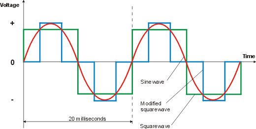
- Modified sine wave inverter gives an output which is intermediate between the square wave and pure sine wave.
- Its actually a sine wave, which has a lot of steps.
- Let's have a look at the below figure:

- In the above figure, the red wave is a pure sine wave and the green signal is a square signal but the blue one is in between and its called modified sine wave.
- Here's a modified sine wave in MATLAB, I have designed it for another project but it will clear the idea How Modified Sine wave looks.
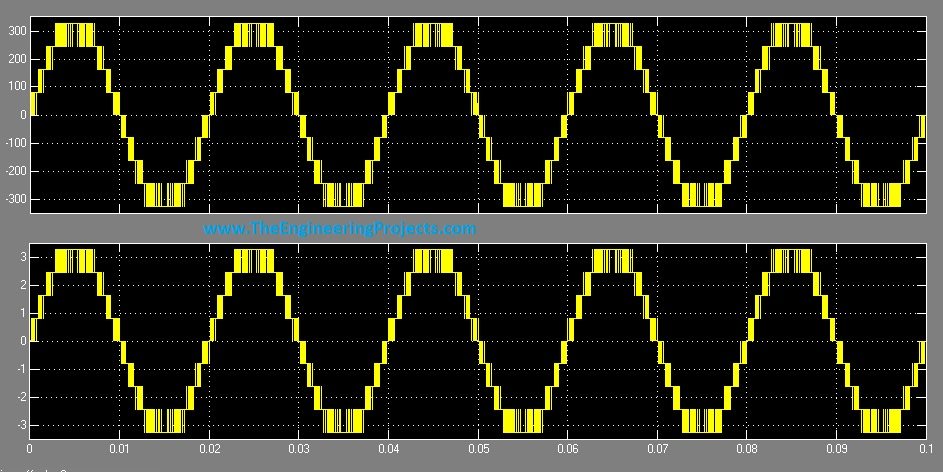
- Modified sine wave has much lower efficiency than the pure sine wave.
- The circuit diagram of a modified sine wave inverter is shown below:

Explanation.
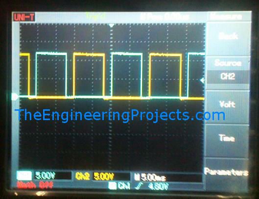
- For a modified sine wave inverter we need two inverted square waves signal to switch the MOSFETs. Two generate these signals we use HEF4047 multi-vibrator IC.
- We use it in a-stable mode. It gives a buffered output so there is no need for impedance matching between TTL based ICs and CMOS based ICs.
- In a-stable mode it generates square wave of exactly 50% duty cycle at its pin 10 and gives its inverted signal on pin 11.
- It also generates frequency double to that of pin 10 at pin 13. It can be done by using 0.2µF capacitor and a 7.6KO resistor as mentioned in its datasheet to generate frequency of 500Hz at pin 13.
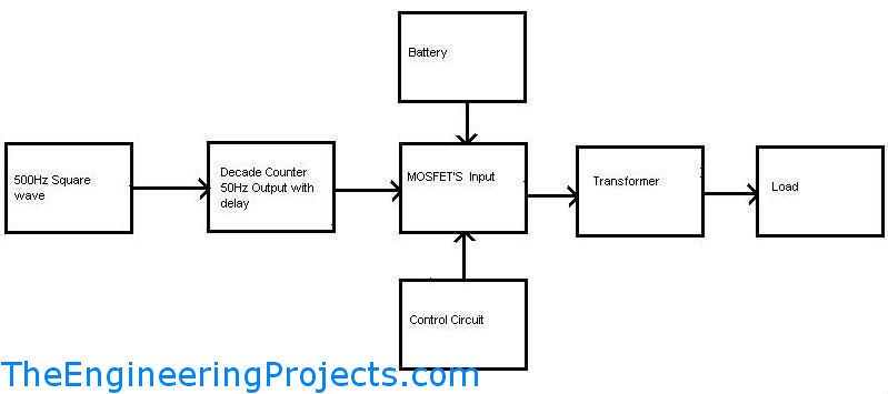
- From pin 13 we give a signal to HCF4017 IC as a clock. HCF 4017 is a decade counter with 12 outputs. It is used to generate a 50Hz signal with controlled delay at both positive and negative edge. Pins 1, 5, 6, 9 and pins 2, 4, 7 are used as output.
- All other outputs are grounded as CMOS ICs are very sensitive and even a small stray signal can burn them out.
- The output of HCF4047 is about 1v, which cannot be used to drive MOSFETs so the signal is amplified by using BC-547 as an amplifier (connected in common emitter biased configuration.
- This signal is again amplified and inverted. The signal obtained is a controlled PWM which we now give at the MOSFET gates.
- The block diagram of the modified sine wave inverter module is given below:
Working
- We gave a PWM signal to the pair of MOSFET connected in a push pull configuration.
- When M1 MOSFET is turned on by a high input (Q), the M2 MOSFET turns off at that time because on its input we had given an inverted signal (Q ) with some delay.
- This delay is used so that one of the MOSFETs gets time to turn off before second one turns on.
- In this mode, the current flows from source to MOSFET M1 as shown in figure.
- When Q1 goes low Q becomes high and M2 turns on, resulting in a current flowing from source as shown in diagram by I2.
- Thus, we get a bipolar high voltage output at the transformers secondary.
- The 22kO resistor from Gate to the source as shown in the diagram is important because when the input signal goes to zero, the MOSFETs may not completely turn off because of the capacitance between gate and source so this resistance makes sure that signal is fully grounded.
- The threshold voltage to turn on a MOSFET is approximately 4V. We are driving MOSFETs with 12v signal so that MOSFETs is completely turned on otherwise it will result in power dissipation.
Results
Problems
- In power inverter, shoot through current is a major problem and needs to be solved.
- It is a short circuit current, and as described in the previous topic, occurs when both MOSFETs are on. This happens for a very short time i.e. for some Nano-seconds.
- But eventually it results in a short circuit current, which causes loading and thus it may damage the MOSFETs.
- This situation can be avoided by introducing a dead time between the two signals both at rise and fall edge.
- If the dead time is increased too much, the output voltages drop because MOSFETs are turned ON for a very short time.
- Finally impedance matching is an important factor.
- Transformers output impedance (Secondary) should be low so that minimum voltage drop occurs when we connect any load to with it.
×
![]()


