Hello friends! Today we will build an LED flashing circuit using a 555 timer in Proteus ISIS. We will start with one LED, calculate its on and off times, and then connect two LEDs so they alternate. No microcontroller program is needed because the timer and its resistor-capacitor network generate the repeating signal.
This is a useful first electronics project because you can see the result while also measuring the signal that produces it. We will connect the circuit step by step, examine the timing capacitor voltage, and compare the calculated period with the waveform in the simulator.
The original diagrams and downloads remain in this tutorial. Some historical connections differ from the recommended arrangement described below, so we will identify those differences explicitly. If you are new to the software, begin with our Proteus ISIS and ARES guide.
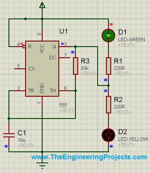
How the 555 Produces a Flashing Output
A 555 can operate in several configurations. In astable mode, it repeatedly charges and discharges a timing capacitor. Two internal comparators monitor that voltage, and the internal latch changes the output state when the relevant threshold is crossed.
With the control pin at its normal level, those thresholds are approximately one-third and two-thirds of the supply voltage. On a 5 V supply, the timing capacitor therefore moves between approximately 1.67 V and 3.33 V during normal repetitive operation.
These levels are fractions of the supply, not fixed 5 V thresholds. This is why the same basic timing principle can work at different permitted supply voltages. The TI NE555 datasheet provides the operating limits, internal behavior and standard astable equations used here.
When the output is high, an LED connected from the output through a resistor to ground can illuminate. When the output is low, that LED turns off. Repeating the charging and discharging process creates the visible flash.
Components and Pin Functions
For the recommended 5 V demonstration, place a 555 model, resistors, capacitors, one or two LEDs, a DC supply and ground. Also add an oscilloscope or voltage probes so that you can inspect the output and timing capacitor rather than relying only on LED animation.
| Pin | Name | Connection or purpose |
|---|---|---|
| 1 | GND | Circuit ground |
| 2 | TRIG | Timing capacitor node, joined to pin 6 |
| 3 | OUT | Flashing output |
| 4 | RESET | Held high for continuous operation |
| 5 | CONT | Control voltage; use a small bypass capacitor to ground |
| 6 | THRES | Timing capacitor node |
| 7 | DISCH | Junction of the two timing resistors |
| 8 | VCC | Positive supply |
The bipolar NE555 and CMOS 555 variants have different supply, current and output characteristics. Select the intended part and read its datasheet before transferring the project to hardware. The numbers below assume a regulated 5 V supply and modest LED current.
Do not confuse a Proteus power terminal with a fully specified real power source. Confirm how the simulation obtains its supply voltage and check it with a probe. An unverified power-net label should not be the basis for an LED-current calculation.
Build the Standard Single-LED Astable
- Connect pins 8 and 4 to the positive supply and pin 1 to ground.
- Join pins 2 and 6 to form the timing node.
- Connect RA from the positive supply to pin 7.
- Connect RB from pin 7 to the timing node.
- Connect timing capacitor C from the timing node to ground.
- Connect pin 3 through an LED resistor and LED to ground, with the LED oriented for current from the output.
- Add approximately 100 nF supply bypassing close to pins 8 and 1 and a typical 10 nF control-pin capacitor from pin 5 to ground.
If C is polarized, its positive terminal belongs at the timing node for this positive-supply circuit. Inspect junction dots carefully. Crossing wires do not always mean connected wires, and a connection to the wrong side of the LED resistor changes the load path.
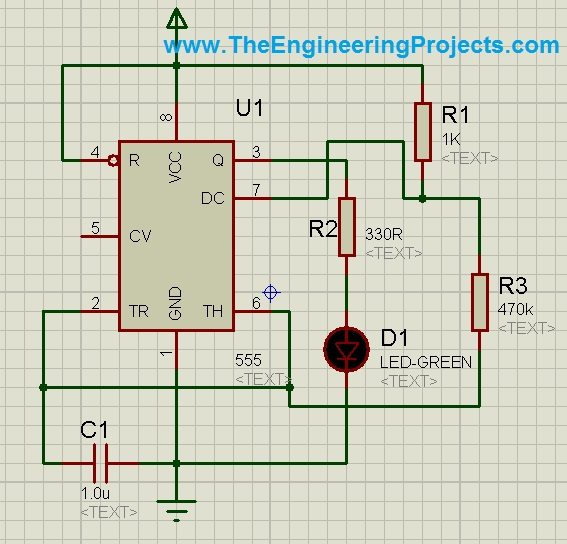
The historical single-LED schematic uses R1 = 1 kΩ, R3 = 470 kΩ and C1 = 1 µF for timing. Its R2 = 330 Ω is the LED resistor, not the second timing resistor. We will use the functional names RA, RB and C to avoid confusing component reference labels with their roles.
The old diagram leaves the control pin without the recommended bypass capacitor and does not show local supply decoupling. Include those components in a physical build. They help prevent supply and control-node disturbances from interfering with the timer.
Calculate the On Time, Off Time and Frequency
In the standard astable, the capacitor charges through both timing resistors but discharges through RB and the internal discharge transistor. The approximate equations are:
- tHIGH = 0.693 × (RA + RB) × C.
- tLOW = 0.693 × RB × C.
- T = 0.693 × (RA + 2RB) × C.
- f = 1 / T.
- High-state duty cycle = tHIGH / T.
Use resistance in ohms and capacitance in farads to obtain seconds. For the original 1 kΩ, 470 kΩ and 1 µF values, the high time is approximately 0.326 s and the low time approximately 0.326 s. The complete cycle is about 0.652 s, giving a frequency near 1.53 Hz.
The original claim that this circuit necessarily stays on for one second does not follow from those values. One complete flash cycle includes both the on and off intervals. State which interval you mean whenever you describe a flashing rate.
A practical approximately one-second cycle
For another example, choose RA = 10 kΩ, RB = 68 kΩ and C = 10 µF. The calculated high time is 0.541 s, the low time is 0.471 s, and the total period is about 1.012 s.
| Quantity | Approximate result |
|---|---|
| Output high time | 0.541 s |
| Output low time | 0.471 s |
| Period | 1.012 s |
| Frequency | 0.989 Hz |
| High-state duty cycle | 53.4 percent |
The standard connection gives a high-state duty cycle greater than 50 percent when RA is positive. Making RA small relative to RB approaches 50 percent, but simply shorting RA is not an acceptable way to obtain it because pin 7 switches toward ground.
Select the LED Resistor
An LED needs a current-limiting resistor. For an output sourcing current, estimate the resistor from R = (VOH − VF) / I, where VOH is the loaded high output voltage and VF is the LED forward voltage at the intended current.
As an initial conservative calculation, assume a maximum 5 V across the series branch and a 2 V LED drop. A 1 kΩ resistor then limits the ideal current to about 3 mA. The real bipolar 555 output may sit below the supply, so the measured current can be lower.
Do not treat the timer's large headline output-current capability as a desirable LED operating current. Modest current is sufficient for a bench indicator and causes less output-voltage drop and supply disturbance. Check the actual LED's forward current and brightness instead of assuming every color behaves identically.
At 3 mA through 1 kΩ, resistor dissipation is I²R = 0.009 W. This is well below a common small resistor's rating under ordinary conditions, but always calculate dissipation again when changing the supply or load. A resistor value suitable for 5 V is not automatically suitable for a higher supply.
Run and Measure the Single-LED Simulation
- Inspect supply polarity, reset and the timing-node connections.
- Start the simulation and wait for several complete cycles.
- Observe the LED and probe pin 3 relative to ground.
- Probe the capacitor node on pins 2 and 6.
- Measure one steady-state high interval, one low interval and their sum.
- Compare the readings with the calculations for the component values actually entered.
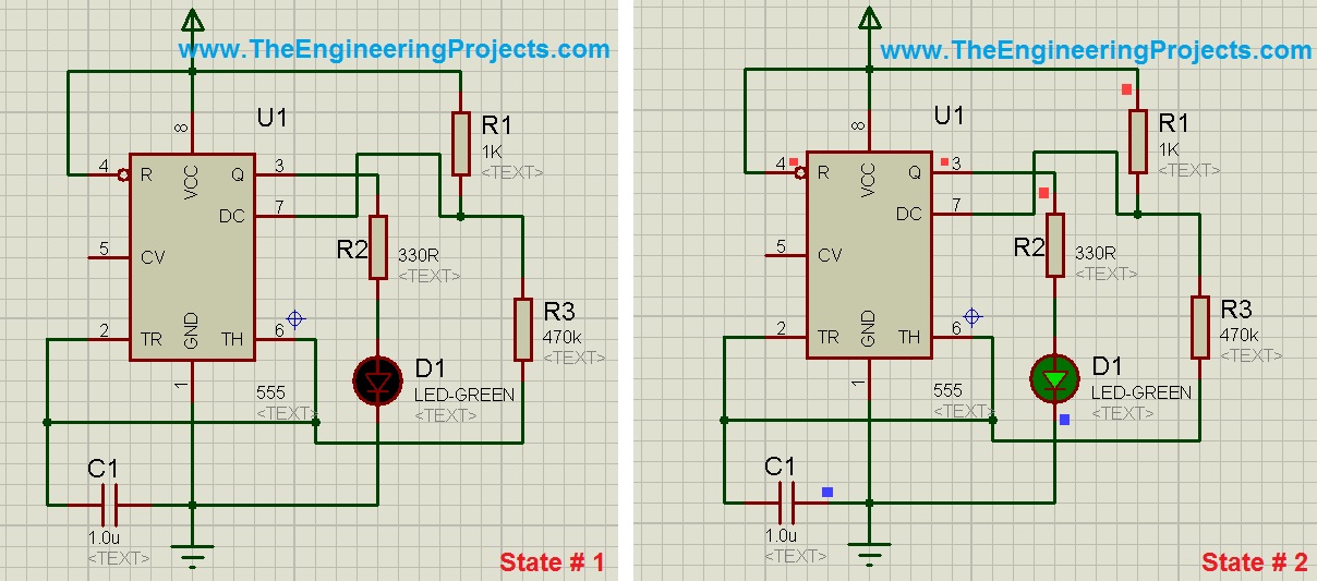
The original image shows the LED in its off and on states. The output should look approximately rectangular while the capacitor voltage rises and falls exponentially between the comparator thresholds. The two waveforms explain the same behavior from different points in the circuit.
The first interval after startup may differ because an initially discharged capacitor starts below the normal lower threshold. Measure later cycles when evaluating the standard astable equations. Also distinguish simulation time from how quickly the animation moves on your computer.
The original single-LED project remains available here. It is an archived example, not a newly rebuilt file containing every wiring recommendation in this revision.
Download Single LED Flashing with 555 Timer in Proteus
Make Two LEDs Alternate
Keep the recommended standard astable and add a second LED branch from the positive supply to the output. That branch has its own resistor, with the LED oriented to conduct when pin 3 sinks current.
| Output state | LED from output to ground | LED from supply to output |
|---|---|---|
| High | Normally on | Normally off |
| Low | Off | On |
Use a separate resistor for each LED and verify both currents. The upper branch sees approximately VCC − VF − VOL when on. The lower branch depends on VOH, so equal resistors do not guarantee exactly equal brightness.
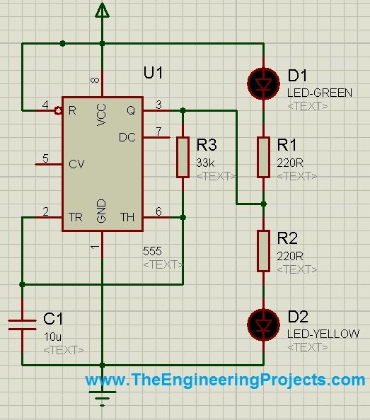
The original double-LED schematic uses a different oscillator: a 33 kΩ resistor feeds the timing capacitor from the output, and pin 7 is left unused. It is not the standard two-resistor astable, so the previous RA/RB equations do not describe it.
That feedback oscillator relies on the loaded output reaching beyond the comparator thresholds. A bipolar 555 sourcing LED current may not provide enough high-level margin at a low supply. For a reproducible beginner build, retain the standard astable described above and change only the two output branches.
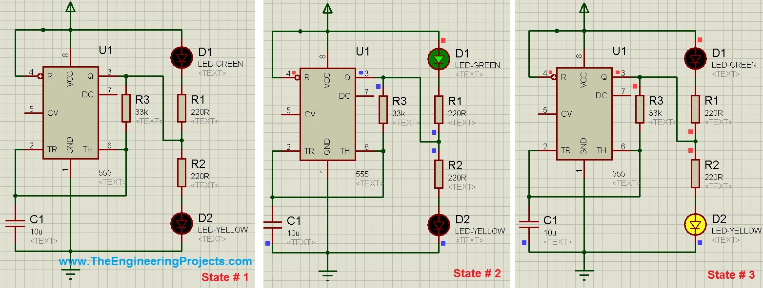
The historical montage includes an initial or stopped condition and two alternating states. Both LEDs being off is not an additional programmed phase of the recommended two-state oscillator. During operation, the intended result is one branch conducting during each output state.
The archived double-LED project is retained for comparison with those original screenshots:
Download 2 Led Flashing Project with 555 Timer in Proteus
Understand Tolerance and Loading
The equations give nominal values. Real resistors, capacitors and threshold voltages have tolerances, and electrolytic capacitor leakage can matter in high-resistance timing networks. A calculated 1.012 s period is therefore not a promise of millisecond accuracy on a breadboard.
For a rough component-only estimate, if both timing resistors scale by +5 percent and the capacitor by +20 percent, the period scales by 1.05 × 1.20 = 1.26. This example shows why a visually acceptable flasher should not be mistaken for a precision time reference.
Loading also matters. Adding many LEDs directly to pin 3 can change the output voltage, heat the device and disturb the supply. A larger display should use appropriate transistor or MOSFET drivers, with separate current limiting for each branch.
Keep the capacitor node away from high-current LED wiring on a physical layout. Place the supply bypass capacitor close to the IC rather than at the far end of a breadboard. These small layout choices help a physical circuit behave more like its idealized schematic.
Why the Timing Equation Contains 0.693
The timing constant comes from capacitor charging between the two comparator thresholds. For a resistor charging a capacitor toward VCC, the remaining difference from VCC decreases exponentially. Starting at VCC/3, that difference is initially 2VCC/3. At the upper threshold of 2VCC/3, the remaining difference is VCC/3.
The remaining difference has therefore halved. The time for that change is RC × ln(2), and ln(2) is approximately 0.693. During charging, R is the sum of the two timing resistors. During discharge toward ground, the capacitor voltage itself falls from two-thirds to one-third of the supply, again halving through RB.
This reasoning also explains the assumptions behind the equations. It treats the thresholds as their nominal fractions, the discharge level as approximately ground, and the capacitor as an ideal component. It does not include every output or leakage effect of a particular device model.
Use reset as a separate control
Pin 4 is an active-low reset input. Pulling it low overrides the normal timing operation and drives the output low. In the single-LED branch connected from output to ground, that turns the LED off. In the alternating circuit, the upper LED may instead turn on because the output is now sinking current.
That distinction is useful when adding an enable switch: resetting the oscillator does not mean that every load connected to it becomes unpowered. If you need both LEDs off, design a separate load-enable function or disconnect their supply through an appropriate switch. Define the desired stopped state before adding control wiring.
Keep reset at a defined high level during ordinary free-running operation. A floating reset wire can pick up disturbances and make the oscillator seem intermittent. Avoid a long unshielded control lead on a breadboard when first checking the timing network.
Record measurements in a small experiment table
For each trial, record RA, RB, C, measured high time, measured low time and supply voltage. Keep the LED load unchanged while changing the timing components. Then restore the original timing values and change the load separately.
This separates timing effects from loading effects. If the period changes after adding LEDs, inspect the supply and waveform amplitudes before concluding that the capacitor changed value. If the capacitor never reaches the upper threshold in the feedback circuit, the missing threshold crossing directly explains why oscillation stops.
Troubleshooting and Review
| Symptom | Check |
|---|---|
| LED always off | LED polarity, supply, resistor path, reset and output voltage |
| LED always on | Timing-node wiring, capacitor connection and discharge path |
| Flashing too fast to see | Capacitance units and resistor values |
| Rate differs from the calculation | Actual topology, entered values, startup interval and component tolerance |
| Unstable hardware behavior | Decoupling, ground connections, supply quality and output loading |
The most informative check is to measure both the output and capacitor voltage. A stationary capacitor voltage points toward the charging or discharge path. A normal timing waveform with a dark LED points toward the LED branch rather than the oscillator.
Once this circuit works, change only C and predict the result before running again. Doubling C approximately doubles both intervals. Then restore C and change RA; notice that the high interval changes while the low interval stays approximately the same. These experiments connect the equations to the circuit.
Frequently Asked Questions
Does this project require code?
No. The 555 and its timing network generate the waveform directly.
Why is the high time longer than the low time?
In the standard astable, charging uses both timing resistors while discharging uses only RB.
Can I omit the LED resistor?
No. The LED branch needs controlled current even if a simulator appears to tolerate an incomplete circuit.
Can I use the original double-LED values in the standard formula?
No. Its output-feedback topology differs from the standard pin-7 astable. Use the appropriate topology and equations together.
What should I learn next?
Explore our 555 timer projects, beginning with output drivers and measured duty cycle before extending the number of LEDs.