 BETA
Power and bypass
Connect V+ (8) to +5 V and V− (4) to ground. Place 100 nF between the rails near the IC.
Build a basic LM358 circuit with labeled pins, component values and connection guidance.
A physical PDIP-8 package, two gain-setting resistors and clear signal wiring.
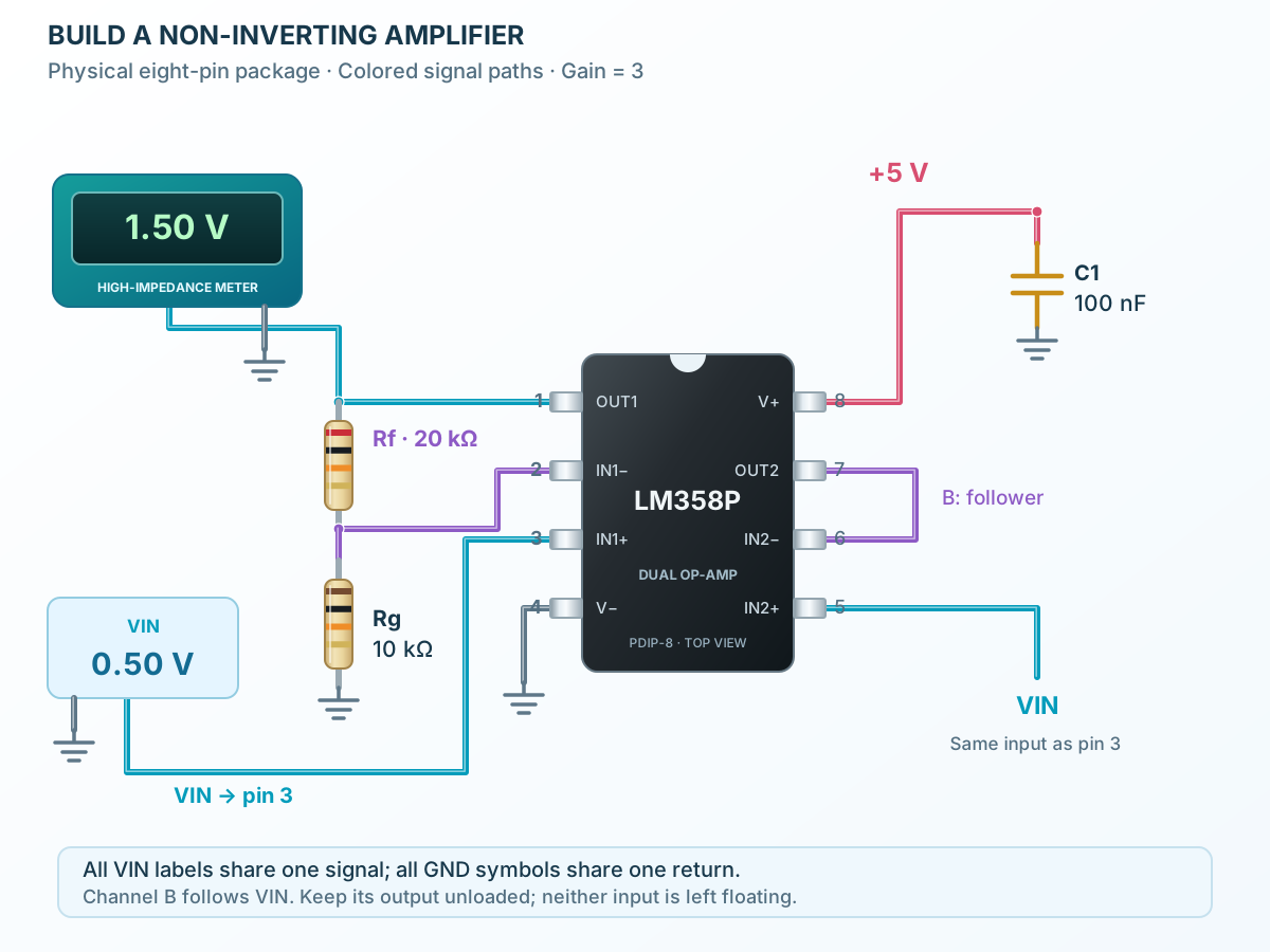
Follow the component values and pin connections
Connect V+ (8) to +5 V and V− (4) to ground. Place 100 nF between the rails near the IC.
Connect VIN to pin 3. Put 20 kΩ between pins 1 and 2, and 10 kΩ from pin 2 to ground. Measure at pin 1.
Connect pin 5 to the same VIN and join pins 6 and 7. Channel B follows VIN with no extra load; its inputs are not left floating.
Change the input and feedback. See the gain and output respond.
Enable JavaScript to explore the amplifier.
Gain = 1 + Rf / Rg · VOUT(ideal) = VIN × Gain
Illustrative DC model at 5 V with a light load: 3.50 V upper output and 0.02 V lower output. Real headroom depends on load, temperature and part variation. Offset, bandwidth, slew rate and noise are omitted; use the ProTech example for a running simulation.