 BETA
MCP3208 Working Principle
Learn how MCP3208 works with an illustrated explanation and practical readings.
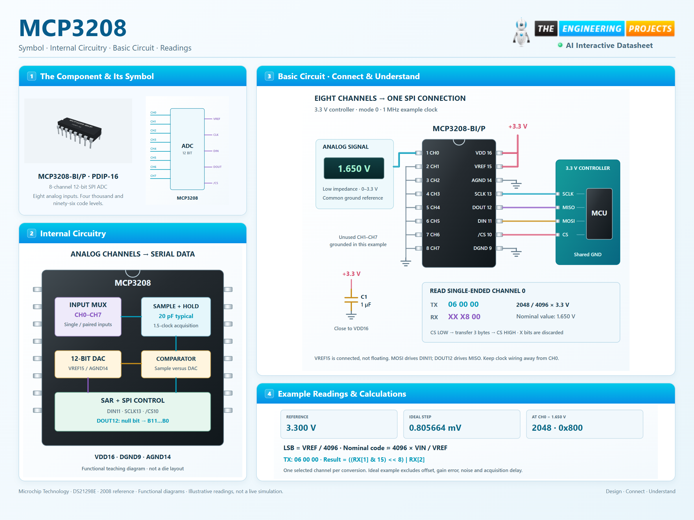
MCP3208 at a glance
Follow the labeled connections and functional stages
How it works
3 stages · Explore one step at a time
Send the input selection
CS LOW starts the transaction. Send START, SGL/DIFF and channel bits D2–D0.
Acquire and approximate
The source charges the sample capacitor over 1.5 clocks. Twelve successive approximation steps resolve the held voltage.
Read the twelve-bit result
Discard the null/framing bits, combine the last four bits of RX1 with RX2, then raise CS.
Choose a channel. Build the SPI message.
Explore 12-bit conversion and single-ended or pseudo-differential inputs.
Channel selection is part of every conversion command. Differential results remain unsigned; a negative difference clips to zero.
06 00 00Three transmit bytes · hexadecimalXX X8 00X = discard · retain 12 result bitsCS pin 10 stays LOW for the transaction. Use SCLK pin 13, mode 0 or 3. Read ((RX[1] & 15) << 8) | RX[2], then raise CS. Ideal MCP3208 code and SPI framing explorer. Rounds to the nearest nominal code and clamps to 0–4095; excludes noise, acquisition delay and offset/gain error. IN− must stay within ±100 mV of ground.