What is Operational Amplifier?

Hello friends, i hope you all are fine and enjoying. Today i am going to explain a very simple but very important tutorial which is named as what is operational amplifier? Operational Amplifier or commonly known as op-amp is a voltage amplifying device. The output of op-amp is much much larger as compared to the potential difference between its input terminals. Operational amplifier has much importance in today's electronic projects and it is also known as a fundamental building block of the analogue electronic circuits. Operational amplifiers were invented a long time ago and they ere also used in computers of old age. In those computers the function of operational amplifiers was to perform mathematical operations.

Operational amplifiers have a large no of applications and are most commonly use to perform some electronic operations like signal conditioning. When signals are transmitted over a long distances and what mostly happens is the strength of the signal is weakened. and some noise and disturbances are also included in it. to overcome these issues, we use repeater circuits and after some times the amplitude of signal is again boosted up with the help of operational amplifier. Similarly op-amp are also used for filtering of the signal. They are also used in logic designed projects to perform mathematical operations like addition, subtraction, integration and differentiation. The reason why operational amplifiers are much popular and are widely used in digital electronic circuits is that, they possess versatility.

Above was a little introduction about operational amplifier, its working and its applications. Now lets explain some other parameters of operational amplifiers which are given as below:

Pin configuration of operational amplifier

Operational Amplifier has major 3 pins. Among these 3 pins, 2 pins are reserved for input and these pins are of much High Impedance. One input of the operational amplifier is known as inverted input and it is marked as negative sign (-) while the other pin of the operational amplifier is known as non-inverting input and it is marked as positive sign (+). Both these inputs have High impedance. The third terminal of the operational amplifier is its output pin and it is of Low impedance. You can also see the pin configuration of op-amp in the feature image of this tutorial.

Characteristics of an op-amp

Operational amplifier is a very important amplifier and used as a building block in various electronics projects. Op-amp possess the following features:

  • The open loop gain of the differential amplifier is Infinite. Formula to calculate gain is:

G = V(out)/V(in)

Now if we are using the operational amplifier in open loop condition then, the input voltages 'V(in)' will becomes zero and the Gain will become infinite.

  • In op-amp there is an input impedance between both terminals of the operational amplifier. In OFF condition, the value of this impedance is much HIGH and mostly it is taken as 'infinite'. The reason to kept such a high value is to permit any current to flow between the input terminals of the op-amp.
  • For a differential operational amplifier input offset voltages are kept zero. This also permits any current to flow.
  • A very important feature of the operational amplifier is that we have a large no of voltage range, which can appear at the output terminal of op-amp. Since op-amp are designed to amplify the voltages up to a wider value, that's why we can say that infinite values of voltages are available at output terminal of operational amplifier.
  • When AC voltages are applied at its input terminals then, op-amp is capable to perform zero shift. Reason is that in electrical, we have various instrument like Transformer, which gives us the phase shift at output voltages. And the output voltages possess a different phase angle as compared to input voltages.
  • Operational amplifier have no impedance connected to its output terminals and we can say that it has zero or negligible impedance.
  • The operation of op-amp is without any kind of noise. The operation of op-amp is noise proof and no problems occurs during its operation.

Operation of Op-Amp

Operational amplifiers have 2 differential inputs which are named as 'Inverting' and 'non-inverting' inputs. In actual case the operational amplifier only amplifies those inputs difference which is applied between its input terminals. The output generated at its terminals can be calculated by the formula given below:

V(out) = G(o.l) {(V+)-(V-)}

  • In the above formula you can see that V(out) represents the output voltages which appears at the output terminal of operational amplifier.
  • G(o.l) is the open loop gain of the operational amplifier.
  • V+ are the voltages applied to the non-inverting input of op-amp.
  • V- are the voltages applied to the inverting input of op-amp. Generally ground is connected at this pin.

Applications of Operational Amplifier

Operational Amplifiers have a large no. of applications and some of them are given below as:
  • Operational amplifiers are widely used in designing of basic and also advanced electronic projects. The use of operational amplifier as a building block in various projects allows us to get our output much pure and cleaner. The word cleaner emphasis on the part that the other circuit elements like resistance, capacitance, inductance etc, effects the output of the circuit and they also distort it.
  • The biggest application of the operational amplifier is 'voltage comparator'. In order to use op-amp as a comparator, we design a circuit without any feedback. To use op-amp as a comparator gives us the opportunity to get wider range of output voltages and also state switching is done in a faster way, which means it can go from ON to OFF state within no time.
  • Op-amp can also be used to design a level detection circuit in terms of voltages. For example if you connect the input or the reference voltages of the  circuit to one of the input of the op-amp then, it will start behaving as an voltage level detection circuit.
  • Op-amp are commonly used in radio transmission circuits. They are able to amplify the output many times, that's why they are preferred for signal transmission.
  •   Op-amp have wide applications in digital electronics and are commonly used to design filter circuits, differential amplifiers and some integration based circuits.
  • Op-amp are also commonly use to design ADC (analog to digital converters) and also DAC (digital to analog converters).
  • Op-amp are used as a major element in designing voltage clamping circuits and oscillators.
  • An interesting application of op-amp is that they are also used to design analogue calculators and some similar electronic products.
Alright friends, that was all from today's tutorial about operational amplifiers. In the coming tutorials, i will also explain some practical applications of operational amplifiers. If you have any questions then, feel free to ask in comments and i will try my best to solve the issue. Till next tutorial Take Care!!! :)

What is 555 Timer?

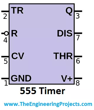
Hello friends, i hope you all are fine and enjoying. Today i am going to share a new tutorial in which I am gonna explain What is 555 timer? We all know about 555 timer, which is an 8-pin IC (integrated circuit), most commonly used in electronic projects, built now a days. As you can see fron its name that it is a timer and designed to generate PWM.

In today's tutorial i am going to explain, what's hidden inside this 555 timer IC and what is 555 timer. A 555 timer is a much compatible electronic device and the biggest feature of this IC is that it able to work on both analogue and digital techniques. Now if we simply consider the output of the 555 timer then, at any particular time, this timer has only 1 definite state. Which means at any time, it will be either ON or OFF. It is not possible that its output is ON and OFF simultaneously. A new invention of 555 timer has also been discovered which is named as 556 timer. 556 is in fact a Dual version of 555 timer and it contains 2 555 timers in a single IC. 556 is a 14 pin IC. Now you will think that 555 timer is a pin IC and as i said that 556 contains two 555 timers then, it should have 16 pins. The answer to this question is that, when two 555 timers are connected to each other then the VCC and GND of both ICs is made common so, we have 14 pins instead of 16. Now let's move towards the basic theme of our tutorial. In this tutorial i will be explain the steps, the pin configuration of 555 timer, It's different modes and project applications.

Internal Design of 555 Timer

Before going into details of what is 555 timer, let's first come to the internal design of a 555 timer. The outer shape of the 555 timer may look like very simple but there is a complex mechanism hidden inside that small IC. A 555 timer contains 25 transistors, 15 resistors and 2 diodes, which are connected to each other in a very complex manner. An interesting thing to know here is that all these components are embedded on a single small silicon chip. Some other series of 555 timers are also available in market like NE555 timer, which we commonly use in our engineering or electronic projects. And the second series is SE555.  SE555 series was designed for military purposes. These operating temperature ranges of both NE555 ans SE555 are given below as:

  • NE555 is mostly used for basic level projects and such high level accuracy is not demanded in it so it is capable to operate from 0 ~ 70 degree Celsius.
  • SE555 was designed for military applications and it is used in those projects where high precision is required. The operating temperature of this IC is -55 ~ +125 degree Celsius.

Pin configuration of 555 Timer

Let's have a look at pin configuration to know what is 555 timer. As I described earlier that 555 timer has total 8 pins. As i described that 555 timer is a multipurpose IC and it is capable to perform variable function. So through some proper arrangement of connections, we can made this IC to do different tasks. Now i will explain the every pin no. and its purpose so that we know the answer to our main question what is 555 Timer ??? :)

  1. The pin designated as pin#1 is GND pin. This pin is used to provide reference voltage or ground to 555 timer.
  2. The pin designated as pin#2 is TR pin. It is used for triggering of 555 timer. The operating voltages of 555 timer is 4.5V ~ 15V. When the operating voltages exceeds 5V then, the 555 timer triggers and it generated output or we can say that now it has crossed that limit above which it will generate output.
  3. The pin designated as pin#3 is the output pin of 555 timer. Through this pin, the output of 555 timer goes to the external circuit. The output depends on the purpose for which you are using 555 timer. For example if you are using your 555 timer to generate PWM then its output will vary. Sometimes it will go High and some time it will go Low.
  4. The pin designated as pin#4 is Reset pin of 555 timer. If you look closely on the first feature image of the tutorial then, you yourself will understand that it is a NOT function. Which means that in order to reset the 555 timer you will have to give '0' at that pin and after the compliment it will become High and 555 timer will 'Reset' .
  5. The pin#5 of 555 is 'CTRL' pin. It is in fact a control pin of 555 timer. This pin gives us the direct access to the internal voltage divider of the 555 timer, which is fabricated inside that small silicon chip. We can divide the voltages according to our output requirements.
  6. The pin#6 is named as 'THR' pin of the 555 timer. For the supply voltages, 555 timer has kept a reference value for them. For example when the supply voltages exceeds 5 volts then, the this pin becomes activated and the 555 timer starts to generate output or it sends data to its output pins.
  7. Pin#7 is named as 'DIS' of the 555 timer. This pin is in fact the discharge pin of 555 timer and used to discharge the capacitors between intervals. This pin has the biggest advantage when, we are generating PWM through 555 timer.
  8. The last pin is pin#8 and it is designated as 'VCC' . This is the supply pin of 555 timer. Source is connected at this pin and as i have already explained that the supply voltages range for 555 timer is 4.5V ~ 15V, but generally it triggers above 5 volts.

Modes of Operation - What is 555 Timer ???

In order to know what is 555 Timer, we should have a look at its modes of operation. 555 timer has 3 major modes of operations. All these modes have there own applications and advantages. All the 3 modes are explained in below:

Astable Mode of 555 timer:

From the name of this mode 'astable mode', you can understand that, in this mode, we don't have any stable output of 555 timer. While operating in this mode, the output will be continuously fluctuating and we will be obtaining a square wave form on the output pin of the 555 timer. To operate the 555 timer in Astable mode, you will have to draw the following circuit, which is shown in the image below:

  • Astable mode is also used to flash lamps and leds. A very similar project named as Sequential LED blinking using 555 timer has also been uploaded by our team. In that project 555 timer was again being used in astable mode.

Monostable Mode of 555 timer:

In this mode of operation the 555 timer gives only one output pulse in addition to the intentional trigger input. For example if you will press the button then, 555 timer will produce a output pulse and its length remains constant until you again press the button and the 555 timer will generate another pulse. The circuit to use 555 timer in monostable mode is shown in the image given below:

  • Monostable mode of 555 timer has wast application. In this state it is used as a timer, touch switches.
  • The biggest example of this mode is to generate PWM. If you recall one of my previous tutorial which was Angle control of servo motor using 555 timer, then at that stage we were using a 555 timer to generate a PWM and through this PWM, we were controlling the angle of micro servo motor.
  • This mode is also used for capacitive measurement and also for missing pulse detection.

Bistable Mode of 555 timer:

The third and the last mode of operation of 555 timer is to use it in bistable mode. This thing is understood from its name 'Bistable' which means this circuit will have 2 stable states, which we are going to control. The circuit diagram to operate a 555 timer in bistable state is shown in the image given below:

  • The above shown circuit is of bistable mode of 555 timer.
  • As you can see in the above figure, we have 2 push buttons. One is connected to 'THR' pin and the other is connected to 'TRIG' pin of 555 timer.
  • When we will press the 'TRIG' button, which means that we have connected the trigger state to ground and its state has become LOW. By doing that the output of 555 timer will become High.
  • On the other hand, when i will press the 'RESET' button then 'THR' pin of 555 timer will be grounded and the output of 555 timer will become LOW.
  • In this way we have made the 555 timer to work in 2 different states and that's why it is called Bistable mode of operation of 555 timer.
If you wanna read more about 555 Timer then you must check below simulations on 555 Timer: Alright friends, that was all from today's post. I hope you have learned something new today and have got your answer for our first question what is 555 timer and if you have any questions then please ask in comments and i will try my best to resolve the issue. Till next tutorial Take Care !!! :)
Syed Zain Nasir

I am Syed Zain Nasir, the founder of <a href=https://www.TheEngineeringProjects.com/>The Engineering Projects</a> (TEP). I am a programmer since 2009 before that I just search things, make small projects and now I am sharing my knowledge through this platform.I also work as a freelancer and did many projects related to programming and electrical circuitry. <a href=https://plus.google.com/+SyedZainNasir/>My Google Profile+</a>

Share
Published by
Syed Zain Nasir