 BETA
Set the gain
Rf = 30 kΩ and Rg = 10 kΩ set a nominal gain of four.
Build a basic LM324 circuit with labeled pins, component values and connection guidance.
A physical 14-pin IC with one amplifier and three defined followers.
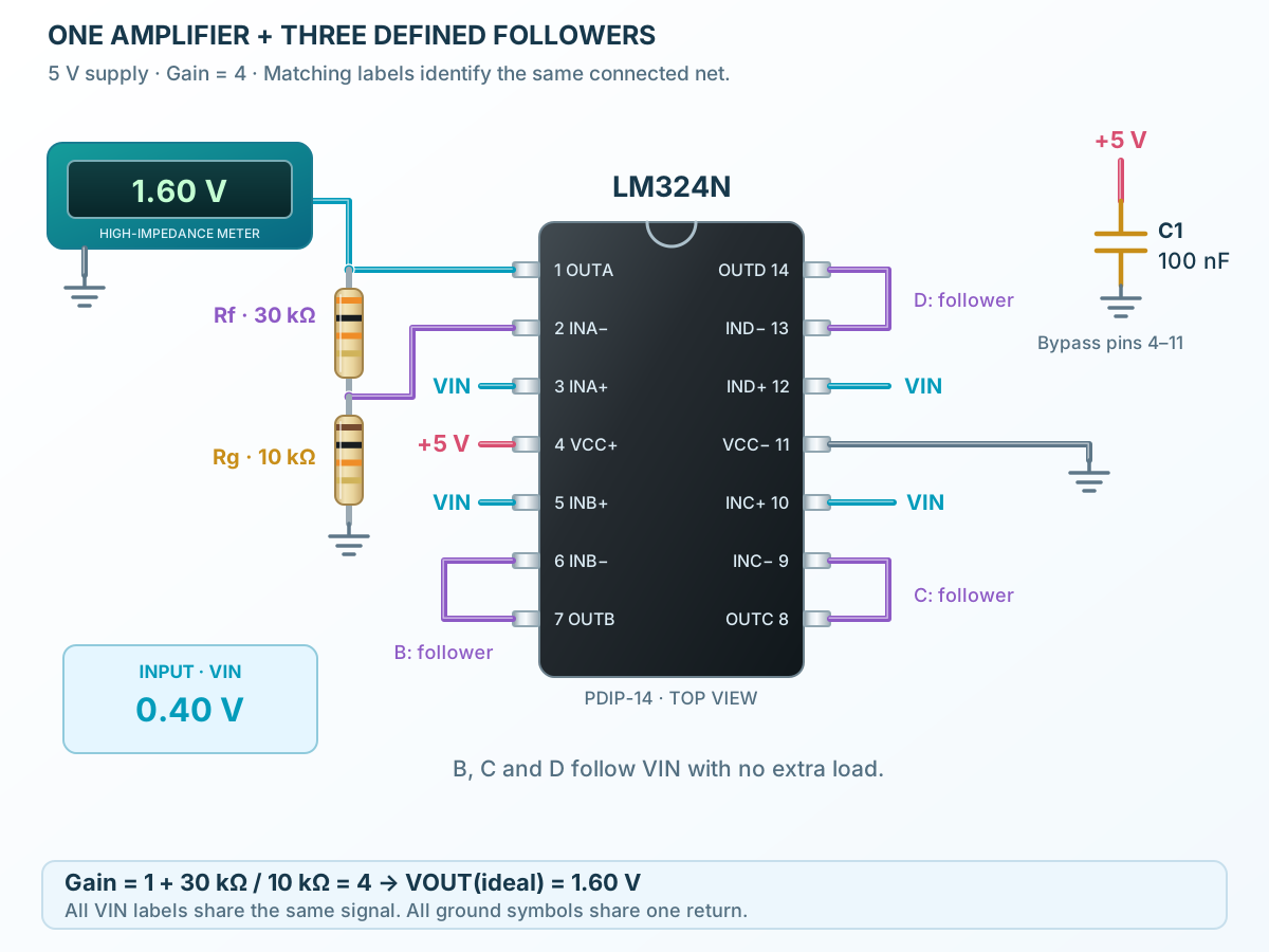
Follow the component values and pin connections
Rf = 30 kΩ and Rg = 10 kΩ set a nominal gain of four.
Channel A amplifies VIN. B, C and D follow VIN, with their outputs connected to their own negative inputs.
0.40 V ideally becomes 1.60 V. Increase VIN in the explorer to see the output approach its estimated upper limit.
Change the input and feedback. See the gain and output respond.
Enable JavaScript to explore the amplifier.
Gain = 1 + Rf / Rg · VOUT(ideal) = VIN × Gain
Illustrative DC model at 5 V and a light load: output limits are estimated at 0.02 V and 3.50 V. Real swing depends on load, temperature and part variation. Offset, bandwidth, slew rate and noise are omitted; this is a teaching explorer rather than a transistor-level simulation.