 BETA
Create the thresholds
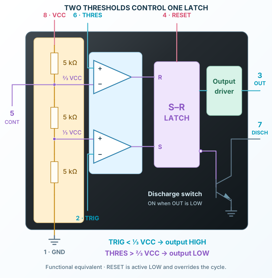
Three nominal 5 kΩ resistors establish 1/3 and 2/3 of VCC. The control pin provides access to the upper reference.
Explore the internal circuitry and functional stages of NE555.
A labeled functional schematic with the important signal paths.
Select a stage to see its role and connections
Three nominal 5 kΩ resistors establish 1/3 and 2/3 of VCC. The control pin provides access to the upper reference.
TRIG below 1/3 VCC sets the latch. THRES above 2/3 VCC resets it. Active-low RESET overrides the timing cycle.
The output stage follows the latch. In the low state, the discharge transistor connects pin 7 toward ground and empties the timing capacitor through RB.