 BETA
Low-power CMOS timer
TLC555 Working Principle
Learn how TLC555 works with an illustrated explanation and practical readings.
Package view
TLC555 at a glance
Follow the labeled connections and functional stages
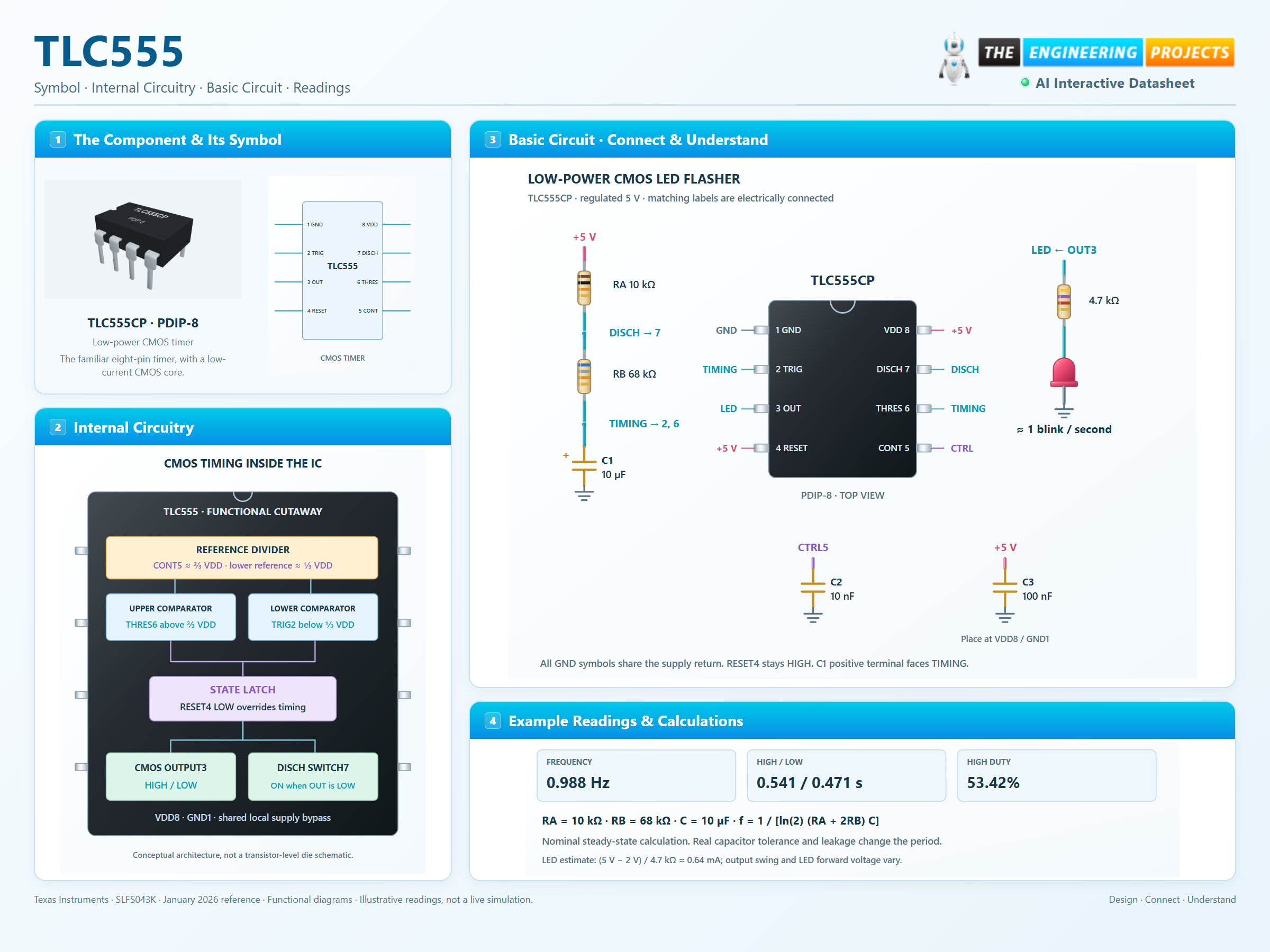
How it works
3 stages · Explore one step at a time
Charge
With DISCH open, the capacitor charges through RA plus RB until THRES crosses the upper threshold.
Discharge
The latch changes state, OUT goes LOW, and DISCH drains the capacitor through RB.
Repeat
When TRIG crosses the lower threshold, the latch sets and the next HIGH interval begins.
Step 1 of 3
Two timing networks. Two waveforms.
Adjust each channel and compare its ideal steady-state timing.
CMOS timer OUT · pin 3
——
——
Supply: 5 V. Each graph uses its own time scale. Nominal astable calculator; not a device simulation. RESET HIGH, CONT unmodulated. Tolerances, startup, leakage and output loading are not modeled.