Hello readers, I hope you all are doing well. Welcome to the Section 2 (ESP32 Features) of the ESP32 Programming Series. ESP32 is equipped with numerous built-in features and in each chapter of this Section 2, we will explore one of these ESP32 features in detail.
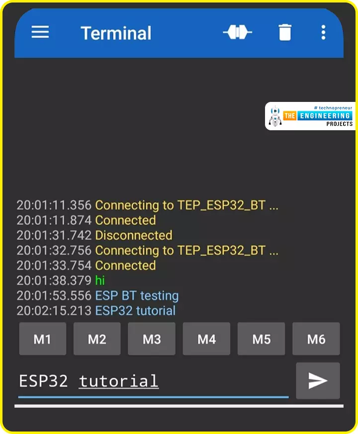
In the previous Section(Section 1: ESP32 IDEs), we installed different software IDEs to program ESP32 boards. Among these IDEs, we are going to use Arduino IDE for programming ESP32. So, I hope all of your tools are configured properly and you are ready to explore the built-in features of ESP32.Today's the 1st Chapter of Section 2, and here we will discuss How to communicate with ESP32 Bluetooth Classic from a smartphone using Arduino IDE.
Here's the video tutorial for ESP32 Bluetooth Classic:
ESP32 Wireless Features ...
Hello geeks, Welcome to our new project. As most readers have already seen the coffee vending machine or maybe you are drinking coffee while reading this article and if you are a tinker or a geek, it must have come to your mind how to make a coffee vending machine on your own. In today's tutorial, we are going to learn how to make a Smart Coffee Vending Machine using Arduino with Proteus Simulation for the same.
We can use this project for an engineering project’s showcase for electronics, electrical engineering students, and can be used in offices as well.
Coffee is the second most popular drink in the world and it is one of the oldest beverages of the world. According to Wikipedia, more than 2 billion cups of coffee are consumed every day in the ...
Hello friends, I hope everything's going well. Today, I am going to share the 13th chapter in the PCB learning series, where we will discuss the single-layer PCB in detail i.e. definition, construction, advantages, manufacturing, applications etc. So let’s try to absorb everything about the single-layer PCB:
Single-layer PCB overview:
Just a quick recall, PCB stands for a printed circuit board having different electrical components connected with the help of pads and tracks of copper foil, incorporated on an insulating material(substrate).
Single-layer PCBs have only one conductive layer of copper. The PCB board itself has a total of 3 layers in single-layer PCB other than the copper layer which are substrate, solder mask, and silkscreen.
In the past, phenolic aldehyde was us ...
An Analog to Digital Converter (ADC) converts a continuous signal (usually a voltage) into a series of discrete values ??(sequences of bits). The main features are:
Resolution (in analog terms): It is the minimum variation of the analog input voltage that can determine the variation of the LSB, that is of the least significant bit of the output code. Since the quantization step Q corresponds to the LSB, it can be said that the resolution coincides with the quantization step Q (and therefore is measured in Volts). We can say that the quantization step Q corresponds to the LSB because two contiguous quantization bands, each of amplitude Q, are identified by codes that differ only for the least significant bit.
Resolution (in digital terms): It is the number n of bits present at the co ...
The SPI (Serial Peripheral Interface) protocol, or rather the SPI interface, was originally devised by Motorola (now Freescale) to support their microprocessors and microcontrollers. Unlike the I2C standard designed by Philips, the SPI interface has never been standardized; nevertheless, it has become a de-facto standard. National Semiconductor has developed a variant of the SPI under the name Microwire bus. The lack of official rules has led to the addition of many features and options that must be appropriately selected and set in order to allow proper communication between the various interconnected devices. The SPI interface describes a single Master single Slave communication and is of the synchronous and full-duplex type. The clock is transmitted with a dedicated line (not necessari ...
EEPROMs (Electrically Erasable Programmable Read-Only Memories) allow the non-volatile storage of application data or the storage of small amounts of data in the event of a power failure. Using external memories that allow you to add storage capacity for all those applications that require data recording. We can choose many types of memories depending on the type of interface and their capacity.
EEPROMs are generally classified and identified based on the type of serial bus they use. The first two digits of the code identify the serial bus used:
Parallel: 28 (for example 28C512) much used in the past but now too large due to having many dedicated pins for parallel transmission
Serial I2C: 24 (for example 24LC256)
Serial SPI: 25 (for example 25AA080A)
Serial - Microwire: 93 (for ...
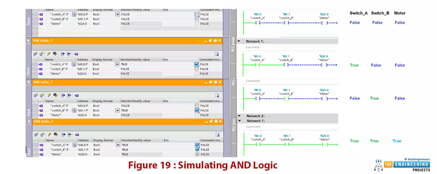
Hello friends, I hope you all are doing great. In today's tutorial, we are going to design logic gates in PLC Simulator. It's our 4th tutorial in Ladder Logic Programming Series. We come today to elaborate the logic gates with comprehensive details for their importance in PLC programming. you can consider logic gates as the building blocks of ladder logic programming. Like every time we start with telling what you guys are going to have after completing this session? For those who like to buy their time and calculate for feasibility, I’d like to say by completing this article, you are going to know everything about what types of logic gates, how they are designed and how they work, how you can translate the logic in your head into the logic gate a ...
Hello friends, I hope you all are doing great. In today's tutorial, I am going to create the first Ladder Logic Program in PLC Simulator. It's 3rd tutorial in our Ladder Logic Programming Series. In our previous tutorial, we have installed PLC Simulator and now we can say our lab is ready to learn and practice. So let us get to work and get familiar with the ladder logic components.
After this article, you will have a complete understanding of PLC contact and coil including their types and possible causes. Because they are the building block of any rung of a ladder logic program. So let us start with ladder logic rung components.
Ladder Logic Contact/Input
In ladder logic programming, a contact represents the input of the system and it could b ...
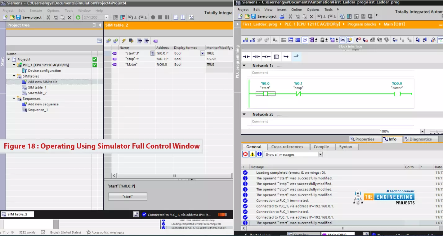
Hello friends, I hope you are doing very well! In today's tutorial, we will set up a simulation environment for Ladder Logic Programming. It's our second tutorial in Ladder Logic Programming Series. In our previous tutorial, we have seen a detailed Introduction to Ladder Logic Programming and we have seen that this programming language is used for PLC controllers.
As PLC is an Industrial Controller, it comes with built-in relays/transistors(with protection circuitry) and thus is quite expensive as compared to microcontrollers/microprocessors i.e. Arduino, Raspberry Pi etc. Moreover, if you are working on a real PLC, you need to do some wiring in order to operate it. So, in order to avoid these PLC issues at the beginning, instead of buying a PLC o ...
Manufactured parts need a quality surface finish and visual appeal before releasing them to the client or market. Although there are different methods of applying the surface finish, anodizing aluminum colors produce the best results.
There is a wide range of aluminum anodizing colors to choose from; therefore, product developers need to know how to color match before releasing the end product. Let’s examine more on anodizing aluminum parts, how to color anodized aluminum and the common anodized aluminum colors.
What is Aluminum Anodizing?
Anodizing is an electrolytic process that produces excellent mechanical properties to enhance aluminum parts' durability and visual appeal. Manufacturers use the anodiz ...