FET: Definition, Symbol, Working, Characteristics, Types & Applications

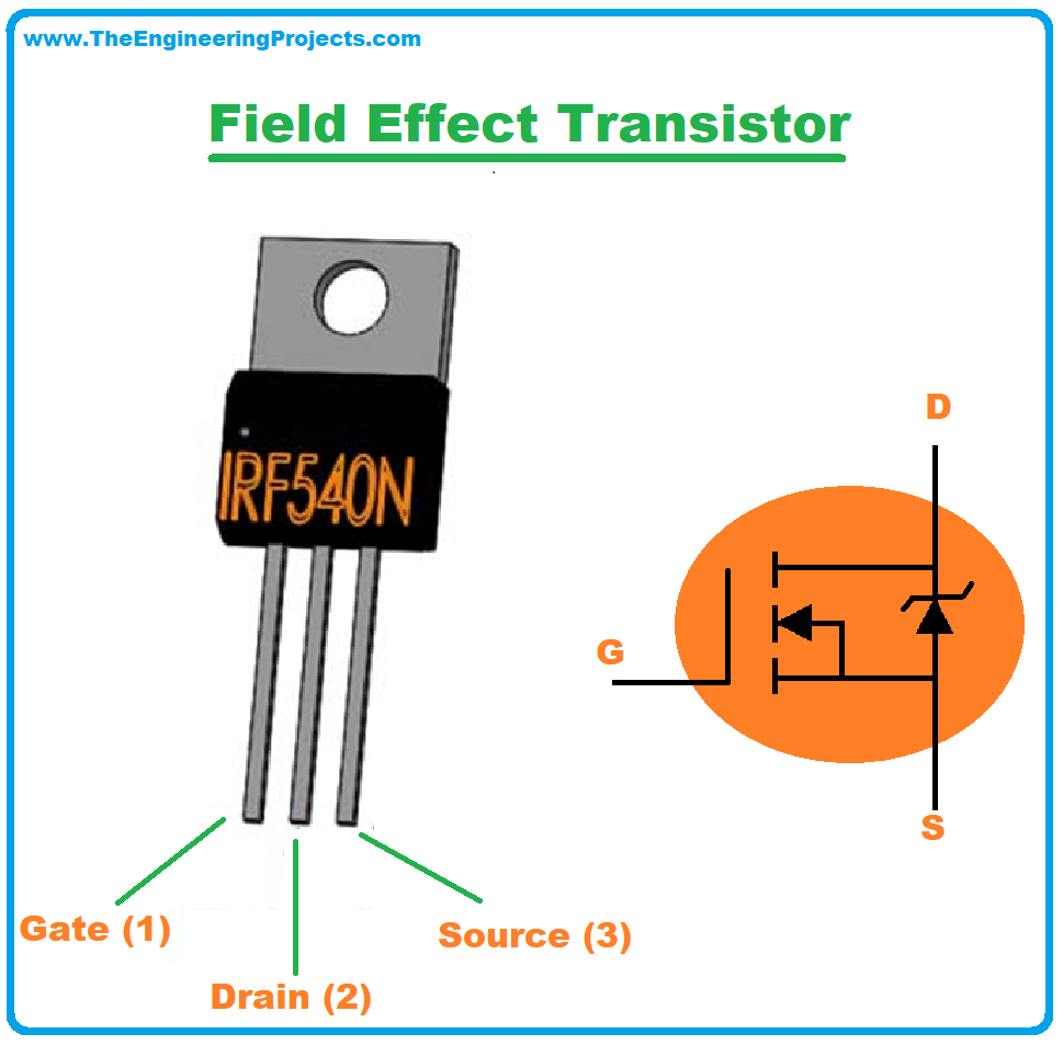
Hello friends, I hope you all are happy, healthy and, content. We have been discussing transistors lately, from the basic definition to the types and characteristics of transistors we have covered it all. If you have a brief idea about transistors, you must be aware of the field effect transistor or you might have heard or read about it somewhere, it is one of the earliest known types of transistors which is our topic of discussion today.
Field Effect Transistors were made to cover up the lacking of previously known transistors which occupied large space and produced a lot of noise, another major problem was the low reliability of previous versions. So, let's get started with the FETs.
Definition of Field Effect Transistor
Let us define field effect transistor first,- "The Field effect transistor is a unipolar transistor made up of semiconductor material, which uses an electric field to control the current flow."
History of Field Effect Transistors
- To know how the field effect transistors evolved throughout the ages, let us have a quick trip to history, the days when we did not have a large amount of resources to materialize our concepts.
- The first attempt to make a field-effect transistor was made by Julius Edgar in 1925, and sadly he failed miserably but he was lucky enough to get the concept patented.
- In 1934, Oscar Heil tried his luck but failed to make a successful attempt.
- In 1945, the Junction field-effect transistor was the first FET device to be constructed by Heinrich Welker.
- In successive years several attempts were made and different types of materials were introduced for making field-effect transistors and their related types. All these successful and unsuccessful attempts led to the formation of the modern-day Field Effect Transistor.
Unipolarity of Field Effect Transistor
Unipolarity of the field effect transistor means that the transistor uses either holes or electrons for working, depending on the type of material being implied for making, unlike the bipolar junction transistors which employ both the electrons and holes for their functioning.
Symbol of Field Effect transistor_ FET
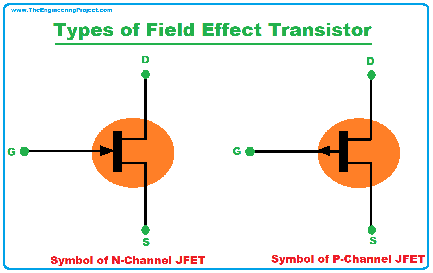
- The following figure shows the symbol of a field effect transistor.
- Three terminals can be seen in the figure namely gate, source, and drain represented by D, G, and S.
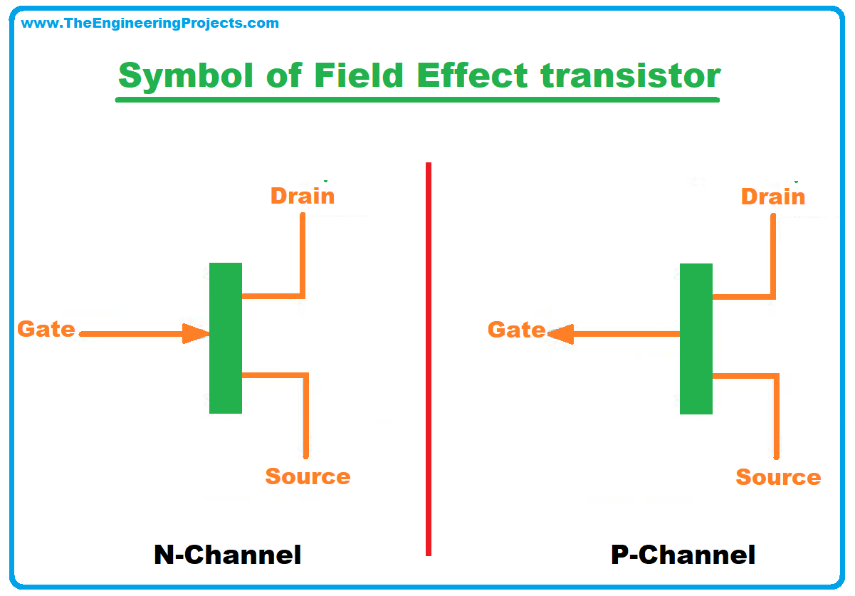
- The direction of the arrowhead reflects the direction of the electric field.
- The symbol is slightly different for two different types of field-effect transistors FETs, they can either be N channel FET or P channel FET, you will learn the symbols of different FETs in their respective sections of this article.
Why Field Effect Transistors are named so, or what is the meaning of FET?
Now you must be thinking about how the field effect transistor got its name? What does it mean by a FET? There are multiple assumptions behind it, the one that I felt to be appropriate is the one that, a weak electrical signal entering through an electrode generates a larger electric field through the other parts of the transistor as well, so they are named field-effect transistors. If you know any other reason, why we call them field effect transistor other than this, you can let me know in the comment section below, I'm looking forward to your response!
BJT vs FET
A lot of times, FET is compared with the BJT let's have a brief overview of their peculiarities in this section. These are some of the significant differences between the two of them;
- BJT is a bit noisy than FET.
- BJT has a higher output impedance than FET.
- BJT is current controlled meanwhile FET is voltage controlled device.
- BJT has a lower input impedance than FET.
Working of Field Effect Transistor FET
Basic construction of a field effect transistor FET
Unlike the other types of transistors, the field effect transistors are not made up of typical collector, emitter, and base, although the number of components is the same but the name and functions of each component are entirely different. To understand the working of the field effect transistor, let us first discuss its basic components one by one.
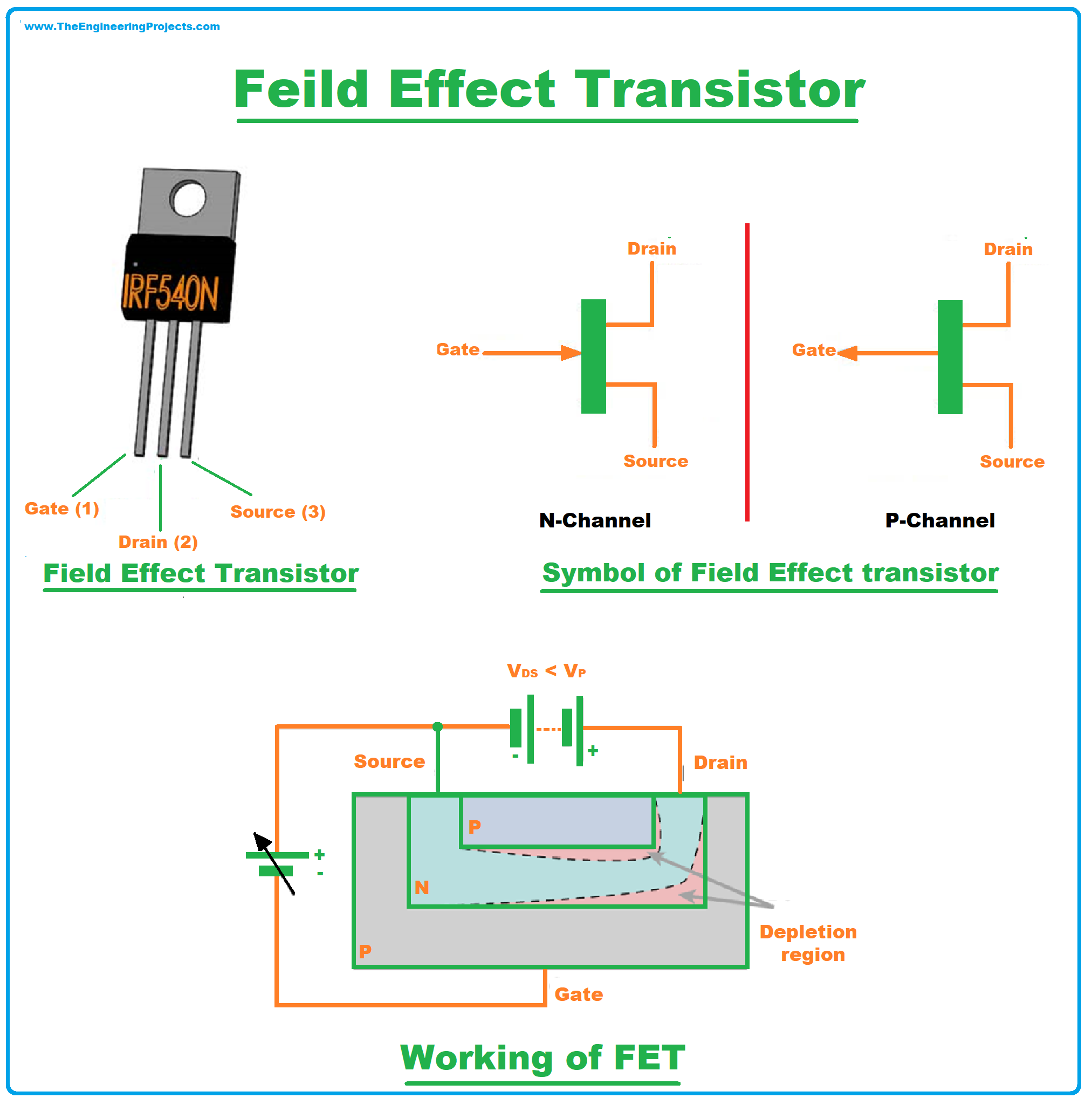
- The source is represented by the symbol S. It acts as an electrode of the field effect transistor through which the charge carriers enter the channel when voltage is applied.
- As the name suggests, the source of a field-effect transistor works as a providing source of charge carriers.
- It is represented by the letter G, wherever you see a G, immediately assume it's a field effect transistor, in the case of transistors. The conductive story of the field effect transistor begins with applying the voltage to the Gate, which is passed on to the other components.
- The drain is represented by symbol D. The drain is the electrode of the field effect transistor which provides the channel to charge carriers helping them leave the circuit.
Working of FET
- As you have a brief idea about the main components of a Field Effect Transistor and their function, we are going to discuss the working of FET.
- The current always flows from the source S towards the Drain D.
- A voltage is applied across the Gate and Source terminal which creates a conductive channel between the source S and Gate G.
- The electrons or holes flow from the source S to Drain D in the form of a stream through the channel.
- There are several other things involved in the working and function of a field effect transistor according to their types, which we are about to discuss in respective sections. So, stay tuned!
- Here arises a simple question which is often left unasked and answered too, why the field effect transistors FETs are called voltage-controlled devices?
- The FETs are called voltage-controlled devices because the current in the drain represented as ID depends on the voltage across the gate G, unlike the bipolar junction transistor which is a current-controlled device.
- The gate voltage is very important for the conduction of current towards the Drain.
- There are two phenomena that influence it one is depletion of the channel and the other is the enhanced state of the channel. Let us discuss them one by one.
- Depletion of channel: Consider an N channel FET, it has the majority of electrons as charge carriers, by making the gate more negative we would repel the electrons from the gate and these electrons would saturate the channel increasing its resistance. This makes the gate region thinner because of the minimal traffic of electrons, but the conduction channel is said to be depleted due to increased resistance.
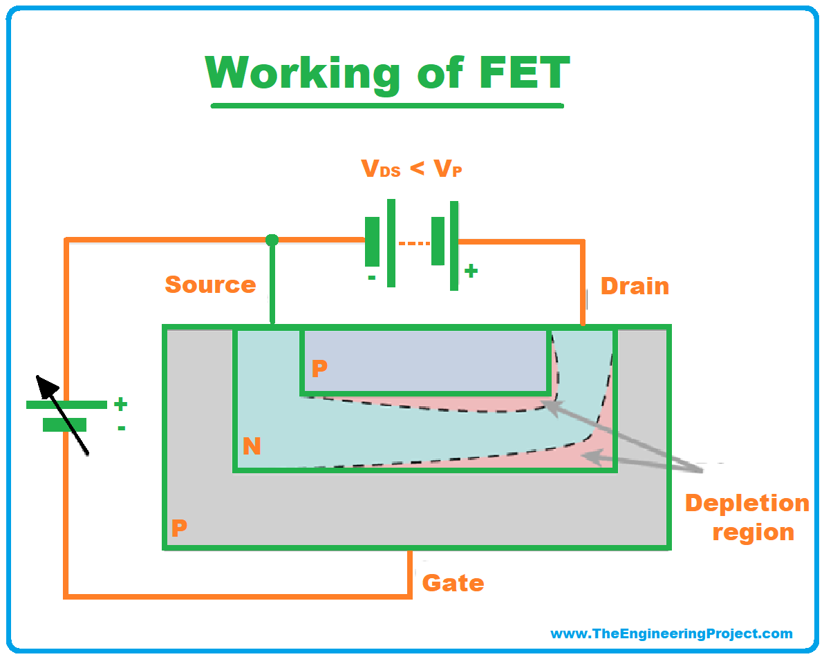
- Again consider the n channel FET, now think yourself, what would happen when you will make the gate G of the FET is more positive? The traffic of electrons would rush towards the gate! It would make the gate region thicker due to greater traffic but on the parallel lines, the conduction channel would be enhanced due to less resistance.
Types of Field Effect Transistor
We can divide the field effect transistor into the following types based on their structure;- Junction Field-effect transistor JFET
- Metal oxide Field Effect Transistor MOSFET
Junction Field-effect transistor JFET
- Junction field effect is one of the simplest types of field effect transistors.
- They are unipolar in function and either work with electrons and holes, the same thing which is peculiar to the simple field effect transistors.
- The junction field-effect transistor has a very high input impedance level.
- Unlike the bipolar junction field-effect transistor, it makes a little noise or is somehow silent as compared to it.
- The structure of the Junction Field-effect transistor is based on its type, in general, JFET is made up of two n-type and one p-type semiconductor material and vice versa.
- The symbol of the junction field effect transistor is as follows;
Types of JFET
There are further two types of junction field effect transistors- N Channel Field Effect Transistors
- P Channel Field Effect Transistors
N Channel Field Effect Transistors
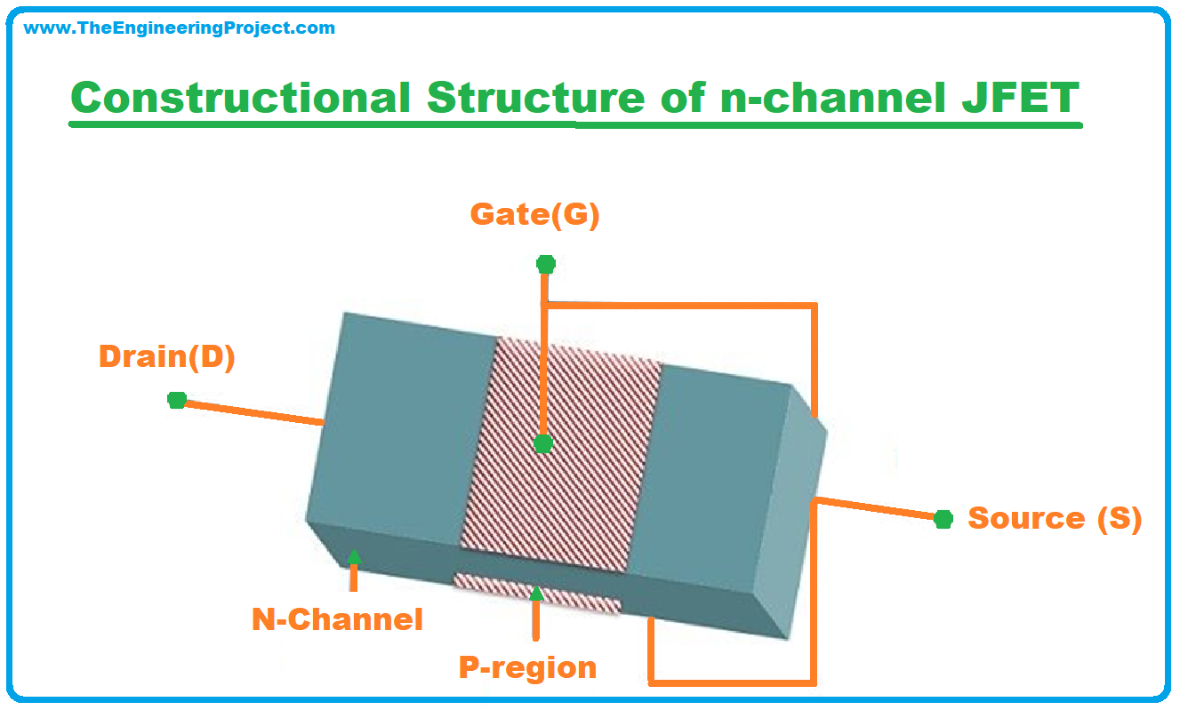
Construction of N Channel FET Let's discuss the construction of N channel Field Effect Transistor first,- A bar of n-type semiconductor material primarily silicone is taken which acts as the substrate.
- The bar is then diffused with two p-type silicone bars which are smaller in size than the n-type silicon bar, on the two extreme ends of the substrate bar. Just imagine you are placing and gluing two small blocks on the extreme right and extreme left sides of a larger block made up of wood or any material you can stick together!
- Now we are done with diffusing the p-type materials into our n-type substrate, the leftover region conducts the current and is labeled as Channel. These channels are responsible for the conductive action of the Field Effect Transistors when voltage is applied.
- After we are done with the formation of the channel, we will now see how the main parts such as Gate, Source, and Drain are formed out of these diffused semiconductor blocks.
- The two diffused p-type silicon bars which have now formed the PN junction with the n-type material are now joined together to form the Gate.
- The two ends of the channel which was formed earlier after the diffusion process are metalized to be converted into source and drain.
- The N channel Field Effect Transistors imply electrons as the majority charge carriers. They are more efficient than the p channel junction Field Effect Transistors because electrons travel faster than the holes.
P channel junction Field Effect Transistors
Construction of P channel FET- The same process is repeated for the construction of the p channel junction Field Effect Transistor.
- The p-type material substrate is taken in form of a large wafer or bar and then diffused with two smaller n-type bars.
- The channel formed after diffusion is then metalized at both ends to form the source and drain.
- The PN junction formed by the two n-type semiconductor materials is then connected to form the Gate.
- So this is how the p channel junction Field Effect Transistors are constructed.
- The p channel junction Field Effect Transistors imply holes as Majority charge carriers as they are unipolar.
Working of Junction Field Effect Transistor
- The Junction Field Effect Transistor always works in reverse biasing condition, that is why they have a very high input impedance.
- In the case of the Junction Field Effect Transistor, the gate current is Zero which is denoted by; IG=0
- The input voltage which is represented by VGS is the controlling factor for the output current which is represented by ID.
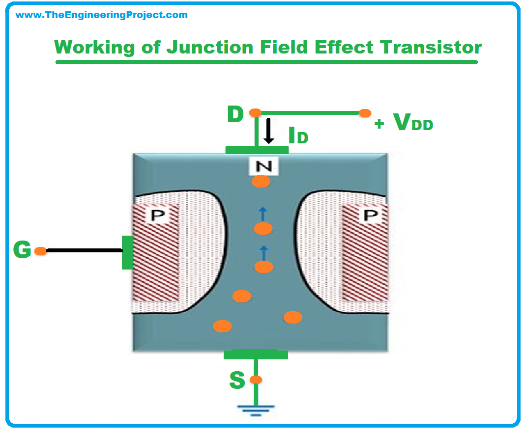
- You must be thinking how we control the width of the channel through which the current is conducted? The answer is simple, we alter the width of the PN junction on both sides of the channel which increases resistance to the flow of current.
As we already know that the Junction Field Effect Transistor only works in reverse biasing conditions let us now discuss a few scenarios to know how the output is generated under different circumstances.
Zero biasing condition of Junction Field Effect Transistor
- When no external voltage VGS is applied to the gate the resulting voltage to the drain would be zero which can be written as VGS = VDS = 0
- The depletion regions would have the same thickness as they had earlier because the voltage is not being applied yet.
- In this zero biased condition the drain current is produced, let me tell you how! The charge carriers in the absence of a potential difference start moving from the source to drain producing a drain current that is opposite to the conventional flow of current.
- So in the zero biased condition, only drain current exists in Junction Field Effect Transistor.
Reverse Biasing condition of Junction Field Effect Transistor
Small Reverse Voltage application scenario- In the presence of a potential or small voltage the gate-source voltage VGS on which the Drain current ID is dependent, on applying small reverse potential width of the depletion region increases.
- Due to the increase in the width of depletion regions on both sides, the channel finds it difficult to conduct current.
- This difficulty of the channel to conduct current results in voltage drop.
- The width of the depletion region increases more towards the drain terminal, one can think of it as accidental but in science, nothing exists within reasoning and logic, the depletion region increases more towards the drain because the voltage drop is higher at the drain side.
- There is a lesser amount of Drain current ID because of the shrinkage of the conduction channel.
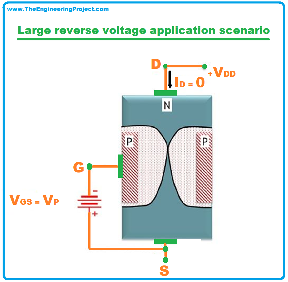
- In this case we apply a higher negative voltage which is our Gate to Source voltage, represented by VGS
- The depletion regions of both the corresponding PN Junctions, keep on increasing in width.
- Eventually, both the depletion regions meet each other or you can say touch each other.
- Here is a question for you, what would happen when both the depletion regions would meet or diffuse into each other? They would eventually block the conduction of the current!
- The point at which the particular voltage blocks the conduction channel completely is called the cut-off voltage or sometimes pinch-off
MOSFET_ metal-oxide field-effect transistors.
The second type of field-effect transistors is the MOSFET, metal-oxide field-effect transistors.
Metal-oxide field-effect transistors are one of the most common types of transistors used widely.
Features of MOSFET
- The MOSFET consumes lesser power than other transistors.
- They are exceptionally scalable and if you remember Moore's law, they are the best practical manifestation of it.
- MOSFETs have high switching speeds that is why they are used for generating pulse trains. Do you know what is a pulse train? A pulse train is the square waveform of asymmetrical waves which are periodic but non-sinusoidal in nature.
- .metal oxide field-effect transistors are considered ideal for digital circuits, analog circuits, and linear circuits as well.
- Sometimes metal-oxide field-effect transistors - MOSFETs are also called IGFET, Insulated Gate Field-Effect Transistors.
Basic Structure of MOSFET
- Let us now discuss the basic structure of metal oxide field-effect transistors MOSFET.
- The metal oxide field effect transistor MOSFET has four components, unlike the JFET.
- The components of MOSFET include Source S, drain D, body B, and Gate G.
- The gate is separated by the body of the transistor through the insulating material
- MOSFET is very similar to the JFET, but the main difference lies in the insulation of Gate Electrode from the conduction channel, either P channel or N channel, with the help of a thin layer of primarily SiO2 or Glass.
- The insulation of the Gate terminal with the metal oxide layer helps in increasing the input resistance. The insulation can increase the value of input resistance into Mega Ohms.
- For a detailed outlook on the MOSFET, its construction, working and applications you can refer to the detailed article present on our website.
Symbol of The metal oxide field effect transistor MOSFET
- The following symbol is used to represent MOSFET.
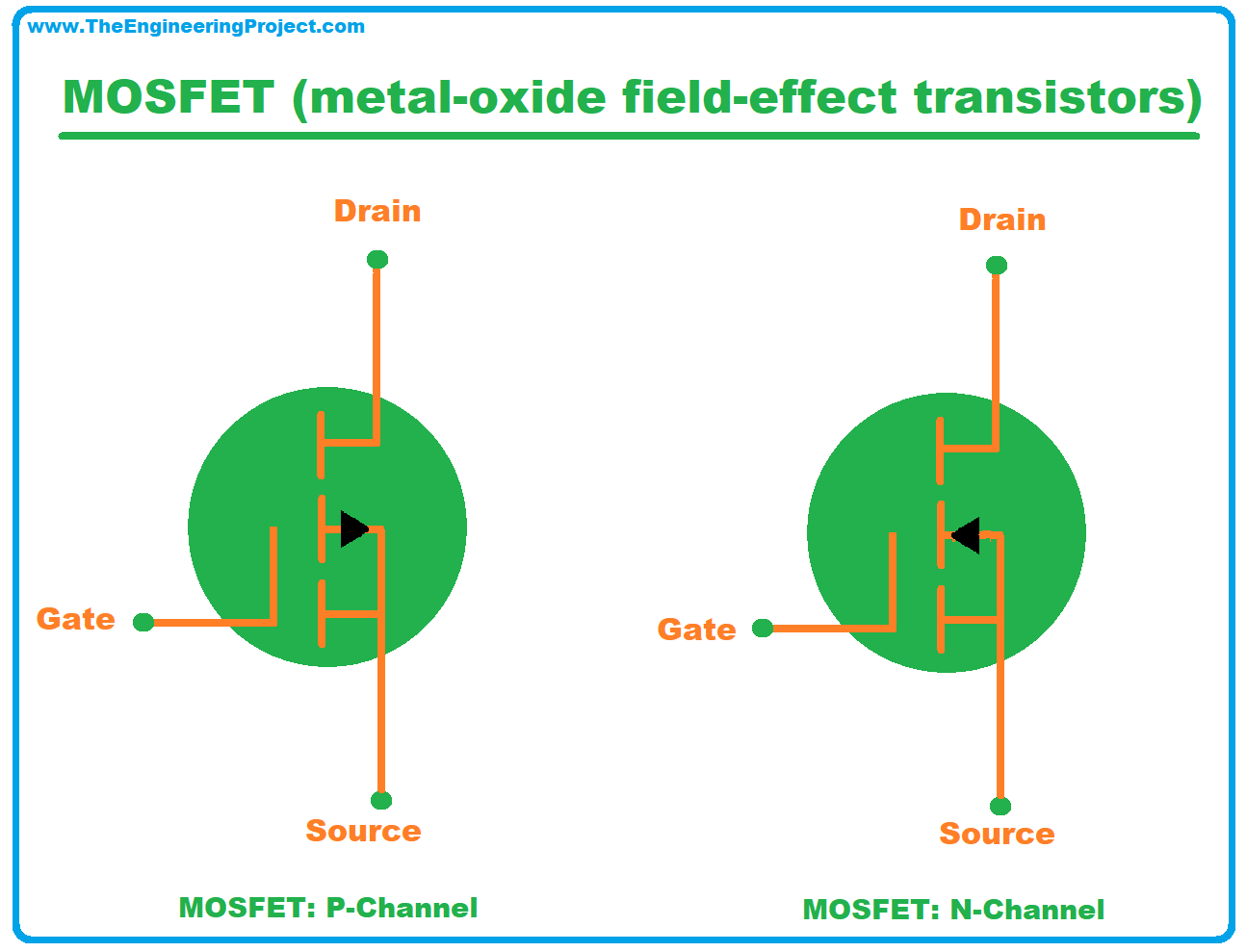
- The Arrowhead indicates the direction of current and I already know that you are aware of this!
- Now you must be thinking, why the symbolic representation is only showing three terminals, please do not search for the fourth one! Because the source is always attached to the body terminal and is represented as one terminal.
- So you can only spot the three terminals naming Gate G, Drain D, and Source S.
Types of MOSFET
Following are the four commonly known types of MOSFET;- N-Channel Enhancement mode MOSFET
- P-Channel Enhancement mode MOSFET
- N-Channel Depletion mode MOSFET
- P-Channel Depletion mode MOSFET
Characteristics of FET
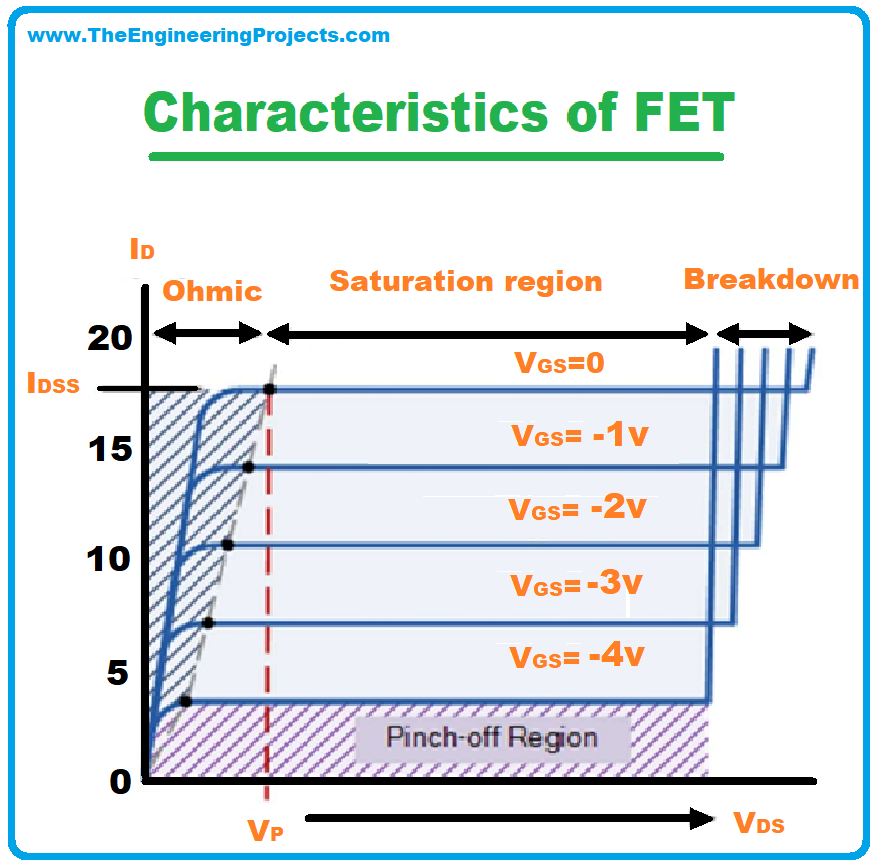
- The Current Voltage, I-V characteristics of the Field Effect Transistor is plotted between the applied voltage VDS and Drain Current ID.
- The graph for studying the characteristic curve of a field effect transistor_ FET is plotted between the varying values of Drain Current represented by ID along the y-axis, with the varying values of VDS along the x- axis.
- Ohmic Region
- Cut off region
- Saturation or Active Region
- Breakdown region
Ohmic Region
- This is the extreme left side of the graph which represents the value of Drain Current ID when the applied voltage of the transistor between the source and gate is Zero i.e VGS= 0
- The conductive channel is small but not narrow in this case.
- Depletion regions on the corresponding sides are equal in size and haven't started expanding yet.
- Our Field effect transistor acts as a voltage controlled resistor at this instance of the IV characteristics curve.
Cut-off Region
- This is the second region of our graph represented by purple the purple lines.
- This cut-off region is also called as pinch-off region because the VGS voltage , the one which controls the current of the transistor is terribly high enough to make the circuit work as an open switch.
- At the pinch off region the conductive channel for current is almost closed due to the Increased thickness of depletion regions on both sides.
Saturation Region
- The saturation region is also called the active region of the graph.
- In this region the Field effect transistor acts a good conductor.
- The value of applied Voltage VGS, the voltage between gate and source drives the transistor.
- The Drain Source Voltage VDS has minimal effect on the current ID of the transistor at this very instant.
Breakdown Region
- This is the last and terminal region of characteristics curve for the field effect transistor, you can observe this region on the extreme right corner.
- The Voltage between the source and drain represented by VDS is very high at this point.
- The voltage is high enough that the conductive channel is broken and maximum current passes through the channel into drain.
Applications of Field Effect Transistors
- Field Effect Transistors have revolutionized the electronic world, there is an endless list of uses of field effect transistors, we are going to discuss a few important ones in this section.
- Field Effect Transistors FETs are frequently used in Integrated Circuits because of their smaller size and compactness.
- FETs are used in operational amplifiers as VRs, Voltage Variable Resistors.
- They are also used in tone controls for mixer operations on TV and on FM as well.
- Field Effect Transistors are also used in logic gates.
- Field Effect Transistors are widely used in the production of digital switches as well.
FET as Buffer Amplifier
- First things first ,let us first discuss what does a buffer do? A buffer makes sure that the signal either digital or analog is successfully transferred to the preceding wave.
- A voltage buffer helps in amplifying the current without disturbing the actual voltage level.
- So, as you are well aware of the function of a buffer, we will discuss how a Field Effect Transistor acts a buffer amplifier.
- A buffer amplifier separates the previous stage of the signal from the next upcoming stage, drain of the Field Effect Transistor works for this purpose.
- Lastly , you must be thinking which characteristic property helps the Field Effect Transistor in achieving this, i have the answer for this question of yours! The high input impedance and low output impedance make a Field Effect Transistor an excellent buffer amplifier.
FET as Analog switch
- We have been discussing the use of Field Effect Transistors in analog and digital switches lately, we will be discussing their use in analog switches now.
- We have discussed it earlier as well in our characteristics curve and operational scenarios of the Field Effect Transistor when the output voltage equals the input voltage making the FET works as a switch.
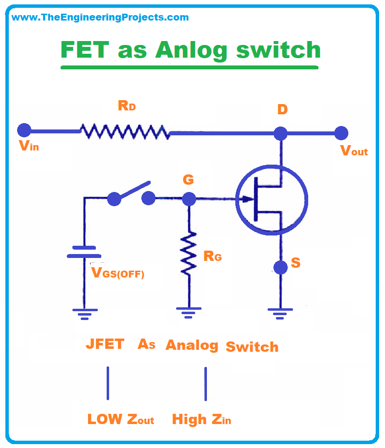
- When the VGS which is the gate source voltage as you already know is absent, the FET works as a small resistance , although a little bit of drain current is present but its value is almost negligible.
- The mathematical expression can be written as
VOUT = {RDS/ (RD + RDS (ON)}* Vin
- If you remember, the cuttoff region of I-V characteristics curve of our Field Effect Transistor, when the max negative voltage is applied to the Gate source region and eventually the Field Effect Transistor_ FET starts acting as a very high resistance.
- That resistance lies in the range of Mega Ohms.
- In this case the output voltage Vout is nearly equal to the input voltage which was VGS.
FET as Phase shift oscillator
- Field Effect Transistors are ideal to be used as phase shift oscillators.
- Phase shift oscillators are used to generate signals with wide range of frequencies.
- Field Effect Transistors can be used for amplifying as well as for feedback loop operation, that is the reason they are excellent to work as phase shift oscillators.
- Field Effect Transistor_ FETs have high input impedance, so there is a very less loading effect when they are used as phase shift oscillators.
- Most of the times N channel JFETs are used for this purpose.
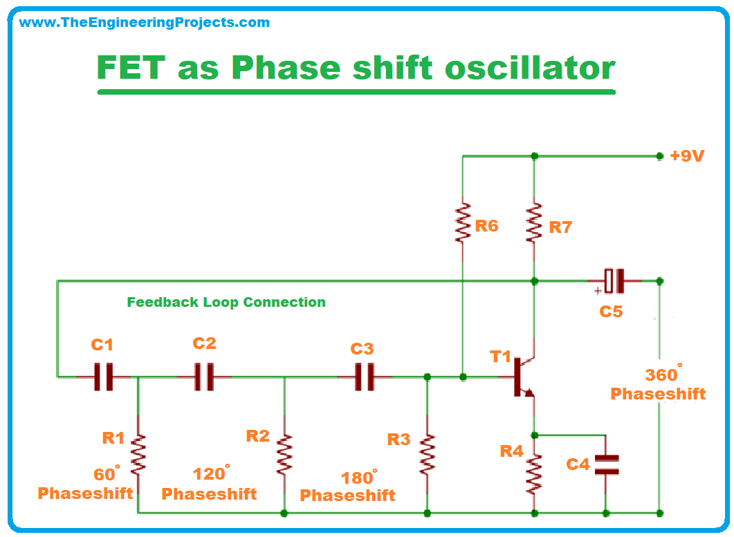
- You can observe the Field Effect Transistors as phase shift oscillators in GPS units, musical instruments and many other places where audio signals are modulated such as voice synthesis.
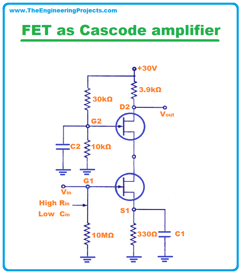
FET as Cascode amplifier
- The word case code has been derived from the phrase " Cascade to Cathode".
- Cascode circuits are made up of two components, the first one is the transconductance amplifier and the second one is the buffer amplifier.
- Cascode amplifiers are generally made using Field-Effect Transistors due to their high input resistance.
- We use cascode amplifiers because of their quality of having low input capacitance, otherwise, the normally used common amplifiers have a higher value of input capacitance in general than the cascode amplifiers.
- Although the voltage gain is the same for both the amplifiers which is again a win-win situation for
- Cascode amplifiers using Field-Effect Transistors.
FET in Multiplexer
- Let us first discuss the function of a multiplexer, a multiplexer collects different signals from different sources to present as a single output signal. Imagine a whole year of hard work and the end result is summarized in a single result card after the exam!
- Junction Field-Effect Transistors are used to construct the multiplexer circuit.
- Each Field Effect Transistor act as an SPST.
- In case you don't know about the SPST, let me tell you, it is the single pole single throw switch that generates one output from one input.
- An SPST is used as an on-off switch in circuits.
- All input signals get blocked when the control signals are made more negative than the Gate source voltage VGS.
- This condition blocks all the input signals.
- By turning any one of the control voltages V1, V2, or V3 to zero we can obtain a single desired output wave.
- Consider if ye turn V2 to Zero we will obtain a triangular signal.
- If we turn V3 to zero, you can yourself figure out from the circuit diagram, the wave signal you would get, Go! Scroll up!
- So this is how the Field Effect Transistors are used in multiplexers.
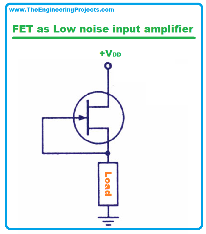
FET as Low noise input amplifier
- How you define noise? A sound that is unpleasant to the ears or when talking of signals a disturbance that causes unnecessary turbulence in the desired output making it meager or weak.
- Noise is produced in many mechanical and electrical instruments but sometimes for a few things it is tolerable and sometimes it is not!
- Just imagine disturbing noise when you are streaming a video or audio, a loud signal which blurs out music during your sunny beach day on your radio, nobody wants that! That is why Field effect transistors are used for low noise amplification.
- Noise has nothing to do with signal strength which is why it is always there, even when you have ended your live stream!
- Noise production is a drawback of many electronic devices but the bright side is that our Field effect transistors make a little less noise especially if they are used in the front end of the signal receiver.
- Field-effect transistors are a bit noisy too, but I have a solution for it, MOSFETs are used where even a little bit of noise can't be tolerated, don't worry we would talk about MOSFETs in our next article!
- So, lastly, we can say that, if we use a Field-effect transistor_ FET on the front end, there is lesser amplification of undesirable signal in our generated output.
FET as Current limiter
- Junction Field Effect transistors can be used to make a current limiting circuit.
- By this characteristic and arrangement, constant-current diodes and current regulators are made, let's discuss the process, but firstly refer to the circuit diagram for better understanding.
- When there is an excess of supply voltage due to any discrepancies in the system, the Junction Field Effect transistor immediately starts operating in its active or saturated region, I hope, by now you are well aware of the active region of the Junction Field Effect transistor, if not, refer to the section of I-V characteristics graph and its explanation!
- At this instance, the Junction Field Effect transistor acts as a source of the current itself and prevents any further load current.
So friends, this last segment concludes our discussion on Field Effect Transistors(FET), I hope you have learned something new from this discussion. For any suggestions or constructive criticism or a little bit of appreciation, you can use the comment section below. See you soon with the next topic, have a good day ahead!


