Semiconductor Materials: Silicon and Beyond

In a number of applications where speed, latency, and light detection are critical, silicon has reached the limits of its capabilities. Global shipments of silicon between 2021 and 2025 are expected to total 17,600 million square inches, according to Statista. It is clear from this report that Moore's law has the potential to last at least until 2025. However, it is also critical to identify a suitable silicon substitute.

Future iterations of the machine will be able to learn from and adapt to its environment thanks to technologies like artificial intelligence. Because of this, more potent and flexible computational processes are required. It is more probable that the production of chips will usher in a new computing revolution. The following are a few possible silicon chip substitutes that could improve computing performance.

Expanding Beyond Silicon as Moore's Law Breaks Through Barriers

University of North Texas, professor Anupama Kaul is setting out on a historic quest to unleash the power of nanomaterials and transform the electronics sector in the cutting-edge field of high-performance computing. Kaul is actively investigating silicon substitutes, tackling issues of national security and inefficiencies with tungsten diselenide as a focus.

Energy inefficiency in the transistor's switching states is currently posing a serious threat to the trillion-dollar silicon electronics sector. According to Kaul, our gadgets, like laptops and iPhones, dissipate a lot of heat. The trillion-dollar electronics industry is powered by silicon, but Moore's Law's limits on transistors scaling and energy inefficiency have put silicon at a critical crossroads.

Kaul's proficiency with two-dimensional layered materials (2DLMs) is evident in this situation. By integrating these materials into chips, she sees a future of computational devices with improved performance and reduced energy consumption. These materials are unique because of their nearly flawless atomic interfaces, which permit electrons to move freely even in nanoscale dimensions without experiencing energy loss or obstructions.

Alternative Materials

As previously observed, even during the early stages of the development of integrated circuit designs, there were always alternatives to silicon available to engineers and inventors. The tech industry, which spent decades and billions of dollars refining the process before reaching a consensus on silicon, is not in a rush to abandon the process and begin the cycle anew with a different material. Whether used in conjunction with silicon or separately, the search continues for an integrated circuit (IC) that is more compact, quicker, more affordable, and, most importantly, uses less power. Researchers are looking into a number of materials, including black phosphorus, graphene, boron nitride nanosheets, and gallium nitride, as potential alternatives to silicon or methods to improve it to boost its transistor-bearing capacity. They are known as 2-D materials because they are thin, flat sheets that are only one or two atoms thick.

The Future Of Semiconductors

Advanced III-V (gallium-nitride) semiconductor electronics, capable of transforming power into high-voltage transmission and vice versa, will serve as the foundation of our future electrical grid. Innovations in III-V materials, such as bismuthides and antimonides, are opening up new applications in medicine, the military, and other civilian fields. They are also opening up new avenues for communication. The exploration of earth-abundant element combinations to create new semiconductors for low-cost, high-efficiency solar cells is ongoing.

And silicon, that old reliable? Its failure to efficiently harness light does not condemn it to the trash heap of history. By developing "silicon photonics," researchers are revitalizing silicon so that it can handle light more effectively than just moving electrons back and forth. One way is to mix tiny amounts of tin, an additional group IV element, with silicon or germanium. As a result, they have altered properties that improve their ability to both emit and absorb light. That tin inclusion turns out to be a challenging task, similar to many other problems in the field of material science.

Conclusion

As we conclude our semiconductor future study, moving past silicon is possible and necessary. Gallium nitride, graphene, and tungsten diselenide are becoming more popular as the tech industry seeks stronger, more flexible materials. These new materials could revolutionize energy efficiency and processing power. Silicon's photonics evolution shows its versatility. This exciting stage of semiconductor development aims to replace outdated technology and reinvent and improve our electronic future by fusing the two.

Ideal diode vs practical Diode

Hello, Students here I am present to cover an article on a series of Electronic devices and circuit theory. The foremost article of this series is Ideal diode vs practical diode. I try to elaborate on basic to modern theory related to the diode. This component act as fundamental to many important circuit devices such as rectifiers, transformers, etc. The question which we cover in this article are;

  • What is a diode?
  • How a diode is formed? Which methodology manufacturer utilized while the formation of the diode?
  • What is the concept of doping and PN junction in diode theory?
  • How does a Diode work?
  • What type of biasing allows a diode to conduct? Under which situation of biasing diode offers a restriction while conducting?
  • Upon which characteristics do we categorize the diode as an ideal diode and practical diode?
  • Which factor makes a diode ideal? And how practical diode is different from an ideal diode?

Along with these questions, numerous questions may arise in your mind related to diode because it is a very vast concept in circuit theory. If you want to know the answer to these questions, keep sticking with our article. The best step taken by our platform for the easiness of our readers is to provide two things in a single platform. A short video of this article is also tried to cover on our YouTube channel. You may visit. The link is given at end of the article.

What is a diode?

A diode is a two-terminal device that worked as a one-way conductor. A diode may assume as a simple solid-state component. This solid-state component is formed when the intrinsic semiconductor such as germanium or silicon Crystal is grown in such a way that one end is doped with pentavalent and the other end is doped with a trivalent impurity. It is also referred to as PN-junction Diode. Here word doped comes from techniques of doping which is used during the manufacturing of diode.

Doping

The process of adding an impurity to an intrinsic semiconductor I.e germanium and silicon. Semiconductors are those materials whose conductivity lies between a conductor ( good to conduct electricity) and an insulator ( bad to conduct electricity). To enhance the conducting capacity of semiconductors they are doped with different Impurities. Here the word impurity is used for those elements which are doped to pure semiconductor, after they are doped the germanium or silicon Crystal no longer remains pure.

Which element is used for doping?

Basically, elements from a fifth and third group of the periodic tables are commonly used in this process. Which refer to as pentavalent impurity (5the group) and trivalent impurity. Byword pentavalent means there are five electrons present in the outermost shell they lose one electron to complete their Octate and to become stable. That’s why these impurities are also named Donor impurity examples of such impurity are phosphorus, bismuth, etc. When we add such impurity to a semiconductor then N-type material is formed. Trivalent are those which have 3 electrons in the outermost shell and they need 1 electron to become stable due to this reason they are also named acceptor impurities. Examples of such impurities are Aluminum, Boron, etc. When they are doped with pure semiconductors then P-type material is formed.

How a diode is formed?

When intrinsic semiconductors is doped with two different Impurities then a junction is formed which I explain you in video of our Engineering prove t channel and I try to explain this also in my article;

When an N-type material is combined with P-type material then a PN junction is formed. In N-type material, there is the availability of a large number of free electrons which act as a majority charge carrier and holes act as minority charge Carriers. While in P-Type materials the doped material belongs to a trivalent group, they need 1 more electron to complete their covalent bond tendency. To complete one hole an electron jump from one shell to another. This creates another hole in the second shell which results in more than holes these holes act as majority charge carrier and electrons act as a minority charge carriers in P-Types material. As soon as these material are combine electrons from the N-side start to attract toward holes in P-side where they both diffuse and as soon as electron diffuse in the P-side this leave behind a positive ion and holes from the P-side move toward N-side and leave behind a negative ion result information depletion layer where there is lack of Carrier but still, there is the availability of negative and positive ions. This creates a natural potential difference between the two sides, thus forming a junction which refer to as PN-junction. Given below energy diagram and other pictorial representation helps to understand my concept.

Symbolic representation of a PN junction diode.

Symbolically a diode is represented as follows: Here N-side of the diode acts as the cathode and the P-side of the diode act as the anode. Current flow in direction to the arrow. There is a positive charge on the p-side and a negative charge on N-side.

How diode works

Under which biasing diode conduct and which biasing make diode poor to Conduct?

Biasing;

Biasing is a process in which to obtain the desire mode of operation we apply potential to both sides of the diode. This potential also helped us to control the width of the depletion layer.

Forward Biasing;

As shown in figure when biasing is applied in such a way that we provide the positive potential to cathode or P-Side of diode which makes it positive and negative potential of battery is connected with N-side of diode this makes the N-side more negative than P-side. This meets the necessary condition for a diode to conduct. This allows the flow of charges with little opposition almost negligible along with the depletion layer which reduces its width. Once a diode starts to conduct, there is slight opposition faced by carriers. This opposition is a referee to as bulk resistance. It combines the resistance of N-type and p-type. Its value is a most 5 ohm or less.

R(B)= R(N) + R(P)

As the value of R(B) is very low therefore there is little voltage drop across the resistance. Thus negligible in circuitry calculations. When the diode conduct fully the forward voltage becomes greater than the barrier potential. Typically the value of barrier potential or forward voltage for silicon and germanium are;

V(f) =0.7V for silicon

V(f)= 0.3V for germanium

Thus we can drive a diode to conduct by making the N-side more negative than the P-side of a diode.

Reverse Bias

When the potential is applied in such a way that the N-side is connected to positive terminal and P-side of diode is connected to the negative terminal of the battery then no electron and hole move through the junction they attracted toward their own attached pole side of the battery thus enhancing the width of depletion layer, junction current becomes reduces to zero. This means that there is large opposition faced by carriers in reverse biasing. However, there is a small few Milliampere current drawn in reverse biased condition due to some thermal agitation process which causes electron and hole pair combination. We can set a reverse biased condition by applying a potential to the N-side such that it drives more positively than the P-side of diode.

The conclusion which we drawn from these two biasing methods is;

Under forward biased conditions n-type is more negative then p-type, depletion layer width, junction Resistance are at minimum value. And device current is at peak value. Under reverse bias every situation becomes reversed p-type is more negative than the n-side. The width of the depletion layer increase and junction resistance meet to peak value we can say it becomes infinite and the device current become negligibly zero.

Want are the characteristics that make a diode ideal?

Ideal diode act as switch. There might be two possibilities which we attain while studying ideal diode. One is open switch and other is close switch. Let’s put a through back on some characteristics which a switch possess:

Ideal diode have following properties, which I also explain in my video whose link is given below of our article source.

Ideal diode can acts as a good conductor and good insulator under varying biasing schemes.

Under reverse biased condition it act as open switch;

In such situation a diode have;
  • Infinite Resistance
  • There is no flow of current across the junction. And diode acts as prefect insulator.
  • All voltage dropped across terminal component.

Under forward biased diode act as close switch

which have following properties;

  • Zero forward resistance
  • Maximum current is dream from diode. AMD Diode acts as perfect conductor.
  • No voltage drop across the components.

Characteristics curve of ideal diode

Now consider a characteristics algorithm for an ideal diode;

Characteristics curve of a circuit is the curve which is dream between the current and voltage to explain the manner in which device work under different situation.

Forward voltage is measured along positive x- axis and reverse voltage along negative x-axis. Similarly forward current and reverse current are measured along positive y-axis and negative y-axis respectively. 1st quadrant represent the forward bias region and 3rd quadrant represent reverse biased operating system. For vertical line in forward bias region the value of forward voltage increases with increase in forward voltage. For horizontal line in reverse bias mode we see that value of reverse current remains at zero level no matter what the value of reverse voltage. This implies diode act as perfect Insulator or open switch under reverse bias condition.

Now we discuss

how practical diode is different from ideal diode and what characteristics it posses?

(a) A practical diode can’t act as a perfect conductor and perfect insulator.

(b)Under reverse bias conditions there are a few milli-ampere current flows. Its value is very low. Now the question is why its Draws a small amount of current when reverse biased, it might be due to some thermal agitation process. Let’s try to explain this query. Consider the characteristics curve of the diode in both situations ideal and practical. in an ideal diode under reverse bias, the curve starts from the origin and there is no reverse current. And knee voltage is zero. Byword knee voltage we consider a point on the current-voltage curve at which there is a sudden increase or decrease of current. When a reverse voltage is increased beyond a limit then a breakdown occurs. Which break the electron-hole pair, and provides us a flow of free charge carrier due to this reason a small current is drawn even under reverse condition for practical diode due to electron-hole pair recombination. The value of knee voltage for silicon PN-junction is 0.7 V.

( c) In an ideal diode under forward biasing there is no voltage drop. While in practical diode there is a finite voltage drop across the terminal component whose value is different for silicon and germanium PN-junction.

(d) Piratical diode offers some finite Resistance under forward biasing which can’t be ignored and under reverse biased conditions there is no infinite Resistance.

The result we obtained about the Practical diode are:

(a) As Long as the knee voltage is not reached, the diode current is zero.

(b) When the knee voltage is achieved the diode begins to work and draws forward current.

Comparison between characteristics curve of ideal diode and practical diode

Lastly, there is an observable difference between the characteristics curve of both diodes.

In an ideal diode for forward biasing the forward current is maximum and the voltage drop is zero. And under reverse conditions no matter what’s the voltage, the reverse current is zero.

While in practical diode under forwarding biased, no current is drawn until the knee voltage that is 0.7 V is reached. Once this voltage is reached and the diode start to conduct the value of knee voltage is approximately equal to forward voltage I.e 0.7 regardless of the value of forwarding current.

The comparison between voltage and current values calculated in both diodes is summarized in below pictorial representation.

Some other considerations which we should make while dealing with practical diode are;

  • Peak reverse voltage
  • Average forward current
  • Forward power dissipation

This is the article from the series of electronic devices and circuit theory. I hope this material might be helpful for you. If you have any queries you may mention your problem in the comment section. Thanks to All.

BJT: Definition, Symbol, Working, Characteristics, Types & Applications

Hello friends, I hope this article finds you happy, healthy, and content. Today, we are about to discuss one of the most commonly known types of transistors which you might have heard of many times when reading about transistors, the transistor under study is none other than the “Bipolar Junction Transistor’’, also known as BJT . In this article, we will go through the basics of the bipolar junction transistor including its meaning ,definition, types, characteristics, and applications. So, let's get started.

Definition of BJT

A BJT in its full form is written as bipolar junction transistor and we can define it as, "A bipolar junction transistor is a three-terminal semiconductor device which is made up of two PN junctions within its structure and is mainly used to amplify current"

History of the bipolar junction transistor_ BJT

  • Prior to the bipolar junction transistors, vacuum tubes were used in electronic circuits which were highly expensive, those too were available in the form of a triode which was a three terminal device like a transistor back then.
  • The vacuum tube triodes remained a hyped-up thing for almost half of a century, but they occupied large space and were less reliable in terms of usage, the other major drawback was the increase in complications related to current, voltage and whatnot just by increasing the number of vacuum triodes in the circuit.
  • So when scientists were done with controlling electrons inside a vacuum tube and its unruly behavior, they started devising other ways to run and control circuits.
  • Finally, in 1947 the efforts of john Walter and Bardeen a rough two-point contact device was made which was nowhere near to the modern of a bipolar junction transistor but it laid the foundation for the construction of a solid-state transistor when previously everything was vacuum!
  • After this not-so-recognized venture, William Shockley made a successful attempt of making a bipolar junction transistor by pressing together the wafers of semiconductor materials.
  • And guess what? William Shockley, John Walter, and Bardeen were awarded with the Noble Prize for their achievements in 1956.
  • The invention of bipolar junction transistors revolutionized the world of electronics beyond imagination.
  • Until the last decades of the 19th century, bipolar junction transistors were manufactured individually as separate components and individual devices but later on, with the invention of integrated circuits, the world saw another electronic revolution.

Features of BJT

Here are some of the peculiar features of bipolar junction transistors;
  • BJT by which we mean bipolar junction transistor is a current-controlled device, you will, later on, get to know how it works. Keep reading!
  • As the name indicates BJT is a bipolar device, which means it uses both the electrons and holes as charge carriers to perform its function.

Symbol of BJT

Bipolar junction Transistor shortly known as BJT has the following three components;
  • Base
  • Emitter
  • Collector
  • All of the three components are represented in the symbol given below as B, E, and E.
Refer to the diagram given below showing the symbol of NPN and PNP Bipolar Junction Transistors;
  • The direction of flow of current is indicated by the direction of Arrowhead.
  • Symbols for different types of BJTs differ accordingly, do not confuse yourself when you see two or more slightly different ones!

Working Principle of a Bipolar Junction Transistor

  • The working principle of both the NPN and PNP transistor is almost the same, both of them differ in the conduction of current through charge carriers based on the majority and minority of charge carriers.
  • The NPN Bipolar junction Transistor has the majority of charge carriers as electrons.
  • The PNP Bipolar junction Transistor has the majority of charge carriers as holes.
  • The current flow is not the result of majority charge carriers despite their quantity, the current flow is due to minority charge carriers in a bipolar junction transistor that is why they are also named as minority carrier devices.
  • The emitter-base junction is always forward biased.
  • The collector-base junction represented by CB is always reverse biased.
  • The Emitter current is written as IE=IB + IC
  • If we consider base current to be very small in actual measurement then we can say that; IE~IC

Types of Bipolar Junction Transistor

As we already know the basic components of the bipolar junction transistor, we would now discuss its type. Bipolar junction Transistor has the following two types;
  • NPN bipolar junction transistor
  • PNP bipolar junction transistor
The image given below shows the types of BJT along with their usage for different purposes; Now we will discuss both of these types in detail.

1. NPN Bipolar Junction Transistor

As the name indicates, in an NPN Bipolar junction Transistor a p-type semiconductor is sandwiched between the two n-type semiconductors just as a cheese slice between two sides of a bun. Refer to the diagram given below for a better understanding; According to the conventional rules when the current moves into a certain component of the transistor it is labeled as positive meanwhile when it leaves the component it is labeled as negative. As we already know, the NPN transistor consists of two PN junctions, made by fusing the two n semiconductors with one p-type semiconductor. The n-type emitter region is heavily doped because it has to pass on charge carriers to the base. The base is not heavily doped and is very thin as compared to the emitter and collector, imagine the size of the cheese slice as compared to the buns! It transfers charge carriers to the corresponding collector. The collector of the NPN transistor is moderately doped and as the name indicates, it collects the charge carriers from the base. Working of NPN Bipolar Junction Transistor
  • Consider the following circuit diagram to understand how an NPN Bipolar junction Transistor works.
  • As already told, the NPN Bipolar Junction Transistor has two PN junctions, so for forward biasing we connect the base-emitter junction with the power supply VBE.
  • The collector-base junction represented by the CE Junction is reverse biased by applying the voltage VCB.
  • The depletion region of the two PN junctions varies in size, do you remember what a depletion region is? In simple words depletion region opposes the flow of current, it acts like a barrier or a block to current flow and is the area where mobile electrons are not present. Have a look at the diagram given below,
  • You must be thinking about why the emitter-base region has a smaller depletion region, meanwhile, the collector-emitter junction has a wider one? Let me solve it for you, It is due to the reason that the base-emitter region is forward-biased!
  • NPN-type Bipolar junction Transistor has a majority of electrons, when the emitter-base junction is forward biased, the electrons start flowing towards the base which is lightly doped, only a few of the electrons would combine with the base holes and the rest of them would then travel to the collector. The current is due to minority charge carriers as we discussed earlier.
  • The current flowing through the emitter-base junction is the emitter current IB, meanwhile, the current flowing through the base is called base current and is represented by IB.
  • Base current IB is very limited as compared to the other types of current present in the circuit.
  • The remaining electrons that missed the recombination pass through the collector-base region to the collector which produces the collector current IC.
  • The emitter current is written as; IE = IB+ IC

PNP bipolar junction transistor

  • PNP bipolar junction transistor is made up of two layers of p-type semiconductor which sandwich the n-type semiconductor layer in between.
  • The entrance for the current is the emitter terminal in the PNP Bipolar Junction Transistor.
  • The emitter-base junction represented by EB is forward-biased in this case.
  • On the parallel lines collector base junction represented by CB is reverse-biased.
  • The emitter current IE is positive meanwhile base current IB and collector current IC are negative.
  • When we talk about the voltage, VEB the emitter-base voltage is positive meanwhile VCB and VCE are negative.
  • NPN and PNP bipolar junction transistors work on the same principle, the only difference they have is of the majority and minority charge carriers. Can you figure out the current flow in a PNP transistor from the image given below?

I-V Characteristics of Bipolar Junction Transistor

To study the input characteristics, output characteristics, and common current characteristics we need to understand the different configurations of bipolar junction transistors. There are three types of configurations for bipolar junction transistors, let's list all three:
  • Common Base configuration
  • Common emitter configuration
  • Common collector configuration
  • First things first, do you have any idea about the characteristics of a Bipolar Junction Transistor, or what are they? And how we determine them? Putting it straight, The I-V characteristics of Bipolar Junction Transistor is simply the graphical manifestation of the current and voltage of a transistor.
  • To study the characteristics cover of the bipolar junction transistor, we will go through the different modes of a Bipolar Junction Transistor which you would be seeing in the curves.

Working Modes of a Bipolar Junction Transistor

There are three dominant regions in which a bipolar junction transistor works;
  • Active region
  • Saturated region
  • Cut off region

Active Region of a Bipolar Junction Transistor

  • In The active region of a bipolar junction transistor in which the collector base region is forward biased meanwhile the emitter base junction is reverse biased.
  • In the active region of a bipolar junction transistor, the transistor works as an amplifier.

Saturated Region of a Bipolar Junction Transistor

In the saturated region the Bipolar Junction Transistor passes a saturated current after reaching a maximal value of threshold voltage. In the saturated region, our bipolar junction transistor works as a switch, an ON switch, and the collector current is fairly equal to the emitter current.

Cut Off Region of a Bipolar Junction Transistor

As the name indicates there is no collector current in the circuit in this region. The transistor is off and the collector is in a reverse-biased state. The image given below reflects the overall voltage story of BJT in different regions; As we are done with the regions and modes in which our Bipolar Junction Transistor works, let us discuss different configurations and their input and output characteristics

Common Base Configuration of a Bipolar Junction Transistor

In the common-base configuration, the base terminal of Bipolar Junction Transistor is connected within the input and output terminals of the transistor.

Input characteristics Common Base Configuration of a Bipolar Junction Transistor

  • The input characteristics are plotted between the emitter current IE and the emitter-base voltage VEB for the varying values of collector-base voltage VCB.
  • We can clearly observe the trend from the graph that, The Emitter base junction is forward biased so the emitter current IE increases with the increasing values of VEB as the collector base Voltage VCB increases.

Output characteristics Common Base Configuration of a Bipolar Junction Transistor

  • The output characteristics of Common Base Configuration of a Bipolar Junction Transistor are plotted between the output voltage VCB and output current IC, follow the graph given below for better understanding;
  • Change in the emitter current IE results in the changing values of collector current IC.
  • The Emitter current IE and Emitter Base Voltage VEB are positive because the region is forward biased.
  • You can observe the active region in the graph, the phase in which the transistor operates at its maximal potential.

Common emitter configuration of a bipolar junction transistor

In the common-emitter configuration of a bipolar junction transistor, the emitter terminal is connected between both the input and output terminals, the thing you already know! Don’t you?

Input characteristics Common emitter configuration of a bipolar junction transistor

  • The graph for the Common emitter configuration of a bipolar junction transistor is plotted between the base current IB and the Base emitter voltage of VBE, for the increasing values of Collector-Emitter voltage, as you can see in the graph plotted below;
  • We can clearly observe from the plotted graph, that the value of base current increases with the increasing value of base-emitter voltage.

Output characteristics Common emitter configuration of a bipolar junction transistor

  • For the common emitter configuration, the output characteristics are plotted between the collector current IC with the varying values of collector-emitter voltage VCE.
  • The graph represents the working of the bipolar junction transistor in three regions namely saturated region, active region, cut off region.
  • The active region is the region in which the current increases with the voltage but it has not reached its maximal value.
  • The saturated region represents the saturated current when the voltage has reached its maximal value. Can you spot all the mentioned regions in the graph given above?
  • In the cut-off region, the emitter region is reverse biased with a minimal amount of current.

Early effect in Bipolar Junction Transistor

  • Here is another important term to be discussed when we are discussing the output characteristics of the bipolar junction transistor which is known as The Early Effect of a bipolar junction transistor, this phenomenon holds an important place when we talk about the I-V characteristics of a bipolar junction transistor. So, without any further delay let's see what is Early Effect in a BJT?
  • As some of you might have presumed Early effect is one of the earlier manifestations of the collector current or anything like this, let me burst your bubble, it is definitely not true! Early effect in the Bipolar Junction Transistor is named after the scientist James M Early.
  • Early effect in the bipolar junction transistor is the change in the effective width of the base region by applying the collector-base voltage VCB.
  • The circuit diagram given below represents the early effect in a bipolar junction transistor;
  • It causes the increase in reverse bias condition of the collector-base junction or in simple words it amplifies the reverse biasing of the collector-base junction causing a considerable decrease in the width of the Base region of the Bipolar junction Transistor.
  • The early effect is fairly important in the output characteristics of common emitter and common collector configuration.
  • Due to the Early Effect in bipolar junction transistor, the Collector Current represented by IC increases by the increasing the Collector-Emitter Voltage VCE.
  • Consider the following graph for better understanding;

Common Collector Configuration of a Bipolar Junction Transistor

You might go through the following names of common collector configuration, we all have nick names and alternate names, and same goes for this configuration;
  • Grounded collector configuration
  • Voltage follower circuit
  • Emitter follower circuit
  • In Common Collector Configuration of a Bipolar Junction Transistor, The collector terminal is kept common within the input and output terminal of the circuit, as we are at the end of our discussion, can you tell which is the input terminal and which one is the output terminal?
  • The input terminal is the place where the input signal for the base is given meanwhile the output terminal is the point where the Output signal is obtained between the collector and the emitter.
  • An important thing to note is that the common collector configuration has very high input impedance.

Input characteristics Common Collector Configuration of a Bipolar Junction Transistor

  • The input characteristics for Common Collector Configuration of a Bipolar Junction Transistor are plotted between the base current IB and Base collector voltage VBC. Refer to the following graph for better understanding,
  • The base current IB is presented on the y axis meanwhile the collector-base voltage VCB is presented on the x-axis.
  • The output voltage VBC increases with the increasing value of IB, you can follow the graph for better understanding.

Output characteristics of Common Collector Configuration of a Bipolar Junction Transistor

  • The output characteristics of the common collector configuration are plotted between the emitter current IE and emitter-collector voltage VCE. Follow the graph for better understanding;
  • The output for the voltage VCE is plotted for different values from zero to the maximal range.
  • You can observe different regions for the output values, such as the Saturation region, Active region, and cut-off region of the graph, I hope by now you have a clear idea what these regions represent. These are the same corresponding values as we studied earlier in the emitter-collector configuration.

Comparison of bipolar junction transistor with other transistors

As we have been discussing the transistors lately, Let us compare bipolar junction transistors with other types of available transistors such as Field-effect transistor FET and MOSFET, metal oxide semiconductor Field-effect transistor. The following section would help you find clear difference between the BJT and FET.

 BJT vs FET/JFET

  • First things first, both of these transistors belong to two different families of the transistor.
  • The bipolar junction transistor as the name clearly indicates is bipolar and JFET/FET is unipolar. If you don't have any idea about the unipolar and bipolar transistors, let me tell you, they are named after the conduction process which involves only one type of charge carriers taking the name of unipolar transistors and the one requiring both types of the charge carriers electrons as well as holes, they are named bipolar transistors.
  • Bipolar Junction Transistor is a current-controlled device meanwhile FET is a voltage-controlled device.
  • Bipolar junction transistors are a bit noisy than FETs.
  • Bipolar junction transistors have higher input impedance than the Field-Effect Transistors.
  • Bipolar junction transistors have lesser thermal stability than the FETs
  • There are three functional components of a bipolar junction transistor named as base, emitter, and collector, meanwhile, FET has different components named as the base, source and drain.
  • Bipolar junction transistors are larger in size than the JFETs.
  •  Bipolar junction transistors is less expensive than the Field effect transistor.
As you might already know that Junction Field Effect Transistors are a type of Field Effect Transistors so I haven’t made a separate heading for the comparison of BJT first with FETs overall and then individually with JFET and MOSFET. Comparison is the thief of joy so this upcoming section about the comparisons of BJTs would be the last one for the Bipolar Junction Transistors, Let’s begin;

 BJT vs MOSFET

Let us now compare bipolar junction transistors with MOSFET;
  • BJT stands for bipolar junction Transistor meanwhile MOSFET stands for Metal Oxide Field-Effect Transistors.
  • A bipolar junction Transistor is a current controlled device meanwhile MOSFET is a Voltage Controlled Device.
  • A bipolar junction Transistor has three components named as emitter-collector and a base, meanwhile, a MOSFET has four components being the body, source, drain, and gate.
  • The output of a Bipolar junction Transistor can be controlled by controlling Base current meanwhile output of a MOSFET can be controlled by controlling Gate voltage.
  • Bipolar junction Transistor has a negative temperature coefficient meanwhile MOSFET has a positive temperature coefficient.
  • Both Bipolar junction transistors and MOSFET are used for switching but the bipolar junction Transistor has a low switching frequency meanwhile MOSFET high switching frequency.
  • Bipolar junction transistor is a bipolar device meanwhile MOSFET is a unipolar device.
  • Bipolar junction Transistor has a high input impedance meanwhile MOSFET has a low input impedance.
  • Bipolar junction Transistors are a bit noisy than MOSFETs.
  • Bipolar junction Transistors are used in low current applications meanwhile MOSFETs are used in high power applications.
  • MOSFETs are preferred for industrial use as compared to bipolar junction transistors because of their higher efficiency.
In case you want a detailed overview on the MOSFET, you can read our detailed article on this topic including definition, types, working and applications.

Applications of the Bipolar Junction Transistor

As we are done with our discussion on the basics and types of bipolar junction transistors let us discuss some of their applications. We already know the bipolar junction transistors are simple and cheaper to manufacture with lesser efficiency than other modern transistors such as MOSFET, there are still some areas where only BJTs are used because as they say old is gold! Let's move to the last segment of our discussion BJTs have countless uses, but here is a brief list for you to go through before we study the detailed applications of Bipolar Junction Transistors through and through;
  • BJT can be used in clipping circuits, for a detailed outlook on this you can read our article on transistors.
  • Bipolar Junction Transistors are used for signal demodulation.
  • We use BJT for amplifying current due to its current gain characteristics.
  • High-frequency applications such as radio frequency also involve Bipolar Junction Transistors.
  • Bipolar Junction Transistors are used for discrete circuit designs because of their easy availability and low-cost manufacturing.
  • Bipolar Junction Transistors are frequently used in analog circuits.
Now it's time to have a detailed discussion on the applications of a bipolar junction transistor;

1. BJT as a Switch

  • You can easily guess how a BJT can work as a switch as we have already discussed its working in detail. Let us go through a brief breakdown of the process;
  • When we have to use a Bipolar Junction Transistor as a switch, we need to keep our circuit on the toes, i.e. we have to constantly alter the current between the saturation phase and the cut off phase of a bipolar junction transistor. Can you recall both the phases? In case you can’t scroll up and read it again.
  • In the cut off phase there is reverse biasing of collector base junction and we do not get any current.
  • Meanwhile in the saturation phase of the Bipolar Junction Transistor it is working on its maximal potential.
  • When the Bipolar Junction Transistor is operational in its Saturation region, there is no voltage drop across the circuit and it is carrying maximal current according to its definite capacity, in this condition we take it as a closed switch.
  • On the parallel lines, in the cut off region, there is no conduction of current due to reverse biasing so we can say that our Bipolar Junction Transistor is working as an open switch.
  • Now you know, how our Bipolar Junction Transistor also known as BJT works as a switch.

2. Bipolar Junction Transistor as Amplifiers

  • If you can recall the characteristics of the bipolar junction transistor you might remember that a BJT acts as an amplifier when it is operated in its saturated region.
  • The current gain of the bipolar junction transistors depends upon the alpha and beta characteristics of the transistor.
  • Due to a huge current gain, the bipolar junction transistor is used in amplifiers in different configurations we have already discussed in detail, can you recall any of them? No worries, I'm listing the three of them again;
  • Common-base configuration
  • Common-emitter configuration
  • Common-collector configuration

3. Bipolar Junction Transistors in Logic Gates

  • Who has not been through the world of logic gates if he or she is somehow related to the world of electronics! I was always in a love-hate relationship with the logic gates.
Emitter Coupled Logic
  • Bipolar junction transistors are a significant part of ECL, emitter-coupled logic.
  • The ECLs are never ever operated in saturated mode, they have a high input impedance and low output impedance.
  • The current keeps on rolling between the ECL pair hence each gate constantly keeps on drawing current, can you think of any of the disadvantages it may cause? Let me solve it for you, The ECL dissipates more energy than the other families of transistors.
  • The Emitter Coupled logic is also named as;
  • Current mode logic CML
  • Current switch emitter follower logic CSEMFL
  • Current Mode logic CML
Fusion of MOSFET and BJT
  • The other new hyped-up thing is the fusion of MOSFET and BJT making a BiCMOS, a bipolar CMOS which reaps the benefits of both, the bipolar junction transistor and MOSFET.
  • In case you are trying to figure out the meaning of that C in BiCMOS, please don't open a new tab, I'll let you know, it stands for Complementary metal-oxide-semiconductor, thank me later!

4. Bipolar junction transistors as logarithmic converter

  • The changes in the junctions of the BJT are logarithmic as we already know that the voltage of our base-emitter changes with the change in the algorithm of our current in the collector-emitter and base-emitter current during different biasing modes.
  • So due to this specialty and predictability in the nature of bipolar junction transistors, we can easily make a BJT to calculate logarithms and anti-logarithms in any circuit.
  • You must be thinking that we can render a diode for this purpose as well, why are we not using a diode instead? The answer lies in the high circuit flexibility and stability of a Bipolar Junction transistor, which a diode can’t provide.

5. Bipolar junction transistors in Temperature Sensors

  • In our previous section, we discussed that the temperature coefficient for the Bipolar Junction transistors is small, so due to this property they can be used as temperature sensors.
  • Now you must be thinking how we can do that practically, there is a simple method to measure the temperature.
  • The base-emitter junction of a BJT has a very stable and predictable current transfer function which depends on temperature, which is why Bipolar Junction transistors are used in Temperature sensors.
  • Following relationships exists between the current and voltage of the two junctions at different temperatures;
In the above-mentioned equation;
  • K is the Boltzmann constant
  • T is the temperature in Calvin
  • VBE is the Base emitter current
  • IC1 and IC2 are the output current at the same temperature on two different junctions.
So friends, this last segment on the applications of BJT concludes our discussion on Bipolar Junction Transistor. I presume you have learned something new from the article, I know some of the portions are a bit difficult to grasp as well especially if you are reading it for the very first time, but don't worry it is not humanly possible to understand everything at once, give it another chance even if it is the bipolar junction transistor or anything else in your life, a second turn never hurts anyone! I'll see you soon with another discussion, Have a good day ahead!

FET: Definition, Symbol, Working, Characteristics, Types & Applications

Hello friends, I hope you all are happy, healthy and, content. We have been discussing transistors lately, from the basic definition to the types and characteristics of transistors we have covered it all. If you have a brief idea about transistors, you must be aware of the field effect transistor or you might have heard or read about it somewhere, it is one of the earliest known types of transistors which is our topic of discussion today.

Field Effect Transistors were made to cover up the lacking of previously known transistors which occupied large space and produced a lot of noise, another major problem was the low reliability of previous versions. So, let's get started with the FETs.

Definition of Field Effect Transistor

Let us define field effect transistor first,
  • "The Field effect transistor is a unipolar transistor made up of semiconductor material, which uses an electric field to control the current flow."

History of Field Effect Transistors

  • To know how the field effect transistors evolved throughout the ages, let us have a quick trip to history, the days when we did not have a large amount of resources to materialize our concepts.
  • The first attempt to make a field-effect transistor was made by Julius Edgar in 1925, and sadly he failed miserably but he was lucky enough to get the concept patented.
  • In 1934, Oscar Heil tried his luck but failed to make a successful attempt.
  • In 1945, the Junction field-effect transistor was the first FET device to be constructed by Heinrich Welker.
  • In successive years several attempts were made and different types of materials were introduced for making field-effect transistors and their related types. All these successful and unsuccessful attempts led to the formation of the modern-day Field Effect Transistor.

Unipolarity of Field Effect Transistor

Unipolarity of the field effect transistor means that the transistor uses either holes or electrons for working, depending on the type of material being implied for making, unlike the bipolar junction transistors which employ both the electrons and holes for their functioning.

Symbol of Field Effect transistor_ FET

  • The following figure shows the symbol of a field effect transistor.
  • Three terminals can be seen in the figure namely gate, source, and drain represented by D, G, and S.
  • The direction of the arrowhead reflects the direction of the electric field.
  • The symbol is slightly different for two different types of field-effect transistors FETs, they can either be N channel FET or P channel FET, you will learn the symbols of different FETs in their respective sections of this article.

Why Field Effect Transistors are named so, or what is the meaning of FET?

Now you must be thinking about how the field effect transistor got its name? What does it mean by a FET? There are multiple assumptions behind it, the one that I felt to be appropriate is the one that, a weak electrical signal entering through an electrode generates a larger electric field through the other parts of the transistor as well, so they are named field-effect transistors. If you know any other reason, why we call them field effect transistor other than this, you can let me know in the comment section below, I'm looking forward to your response!

BJT vs FET

A lot of times, FET is compared with the BJT let's have a brief overview of their peculiarities in this section. These are some of the significant differences between the two of them;

  • BJT is a bit noisy than FET.
  • BJT has a higher output impedance than FET.
  • BJT is current controlled meanwhile FET is voltage controlled device.
  • BJT has a lower input impedance than FET.

Working of Field Effect Transistor FET

Basic construction of a field effect transistor FET

Unlike the other types of transistors, the field effect transistors are not made up of typical collector, emitter, and base, although the number of components is the same but the name and functions of each component are entirely different. To understand the working of the field effect transistor, let us first discuss its basic components one by one.

Source
  • The source is represented by the symbol S. It acts as an electrode of the field effect transistor through which the charge carriers enter the channel when voltage is applied.
  • As the name suggests, the source of a field-effect transistor works as a providing source of charge carriers.
Gate
  • It is represented by the letter G, wherever you see a G, immediately assume it's a field effect transistor, in the case of transistors. The conductive story of the field effect transistor begins with applying the voltage to the Gate, which is passed on to the other components.
Drain
  • The drain is represented by symbol D. The drain is the electrode of the field effect transistor which provides the channel to charge carriers helping them leave the circuit.

Working of FET

  • As you have a brief idea about the main components of a Field Effect Transistor and their function, we are going to discuss the working of FET.
  • The current always flows from the source S towards the Drain D.
  • A voltage is applied across the Gate and Source terminal which creates a conductive channel between the source S and Gate G.
  • The electrons or holes flow from the source S to Drain D in the form of a stream through the channel.
  • There are several other things involved in the working and function of a field effect transistor according to their types, which we are about to discuss in respective sections. So, stay tuned!
  • Here arises a simple question which is often left unasked and answered too, why the field effect transistors FETs are called voltage-controlled devices?
  • The FETs are called voltage-controlled devices because the current in the drain represented as ID depends on the voltage across the gate G, unlike the bipolar junction transistor which is a current-controlled device.
  • The gate voltage is very important for the conduction of current towards the Drain.
  • There are two phenomena that influence it one is depletion of the channel and the other is the enhanced state of the channel. Let us discuss them one by one.
  • Depletion of channel: Consider an N channel FET, it has the majority of electrons as charge carriers, by making the gate more negative we would repel the electrons from the gate and these electrons would saturate the channel increasing its resistance. This makes the gate region thinner because of the minimal traffic of electrons, but the conduction channel is said to be depleted due to increased resistance.
  • Again consider the n channel FET, now think yourself, what would happen when you will make the gate G of the FET is more positive? The traffic of electrons would rush towards the gate! It would make the gate region thicker due to greater traffic but on the parallel lines, the conduction channel would be enhanced due to less resistance.

Types of Field Effect Transistor

We can divide the field effect transistor into the following types based on their structure;
  • Junction Field-effect transistor JFET
  • Metal oxide Field Effect Transistor MOSFET

Junction Field-effect transistor JFET

  • Junction field effect is one of the simplest types of field effect transistors.
  • They are unipolar in function and either work with electrons and holes, the same thing which is peculiar to the simple field effect transistors.
  • The junction field-effect transistor has a very high input impedance level.
  • Unlike the bipolar junction field-effect transistor, it makes a little noise or is somehow silent as compared to it.
  • The structure of the Junction Field-effect transistor is based on its type, in general, JFET is made up of two n-type and one p-type semiconductor material and vice versa.
  • The symbol of the junction field effect transistor is as follows;

Types of JFET

There are further two types of junction field effect transistors
  • N Channel Field Effect Transistors
  • P Channel Field Effect Transistors
We will now discuss these two types of junction Field Effect Transistors - JFET in detail.

N Channel Field Effect Transistors

Construction of N Channel FET Let's discuss the construction of N channel Field Effect Transistor first,
  • A bar of n-type semiconductor material primarily silicone is taken which acts as the substrate.
  • The bar is then diffused with two p-type silicone bars which are smaller in size than the n-type silicon bar, on the two extreme ends of the substrate bar. Just imagine you are placing and gluing two small blocks on the extreme right and extreme left sides of a larger block made up of wood or any material you can stick together!
  • Now we are done with diffusing the p-type materials into our n-type substrate, the leftover region conducts the current and is labeled as Channel. These channels are responsible for the conductive action of the Field Effect Transistors when voltage is applied.
  • After we are done with the formation of the channel, we will now see how the main parts such as Gate, Source, and Drain are formed out of these diffused semiconductor blocks.
  • The two diffused p-type silicon bars which have now formed the PN junction with the n-type material are now joined together to form the Gate.
  • The two ends of the channel which was formed earlier after the diffusion process are metalized to be converted into source and drain.
  • The N channel Field Effect Transistors imply electrons as the majority charge carriers. They are more efficient than the p channel junction Field Effect Transistors because electrons travel faster than the holes.

P channel junction Field Effect Transistors

Construction of P channel FET
  • The same process is repeated for the construction of the p channel junction Field Effect Transistor.
  • The p-type material substrate is taken in form of a large wafer or bar and then diffused with two smaller n-type bars.
  • The channel formed after diffusion is then metalized at both ends to form the source and drain.
  • The PN junction formed by the two n-type semiconductor materials is then connected to form the Gate.
  • So this is how the p channel junction Field Effect Transistors are constructed.
  • The p channel junction Field Effect Transistors imply holes as Majority charge carriers as they are unipolar.

Working of Junction Field Effect Transistor

  • The Junction Field Effect Transistor always works in reverse biasing condition, that is why they have a very high input impedance.
  • In the case of the Junction Field Effect Transistor, the gate current is Zero which is denoted by; IG=0
  • The input voltage which is represented by VGS is the controlling factor for the output current which is represented by ID.
  • You must be thinking how we control the width of the channel through which the current is conducted? The answer is simple, we alter the width of the PN junction on both sides of the channel which increases resistance to the flow of current.

As we already know that the Junction Field Effect Transistor only works in reverse biasing conditions let us now discuss a few scenarios to know how the output is generated under different circumstances.

Zero biasing condition of Junction Field Effect Transistor

  • When no external voltage VGS is applied to the gate the resulting voltage to the drain would be zero which can be written as VGS = VDS = 0
  • The depletion regions would have the same thickness as they had earlier because the voltage is not being applied yet.
  • In this zero biased condition the drain current is produced, let me tell you how! The charge carriers in the absence of a potential difference start moving from the source to drain producing a drain current that is opposite to the conventional flow of current.
  • So in the zero biased condition, only drain current exists in Junction Field Effect Transistor.

Reverse Biasing condition of Junction Field Effect Transistor

Small Reverse Voltage application scenario
  • In the presence of a potential or small voltage the gate-source voltage VGS on which the Drain current ID is dependent, on applying small reverse potential width of the depletion region increases.
  • Due to the increase in the width of depletion regions on both sides, the channel finds it difficult to conduct current.
  • This difficulty of the channel to conduct current results in voltage drop.
  • The width of the depletion region increases more towards the drain terminal, one can think of it as accidental but in science, nothing exists within reasoning and logic, the depletion region increases more towards the drain because the voltage drop is higher at the drain side.
  • There is a lesser amount of Drain current ID because of the shrinkage of the conduction channel.
Large reverse voltage application scenario
  • In this case we apply a higher negative voltage which is our Gate to Source voltage, represented by VGS
  • The depletion regions of both the corresponding PN Junctions, keep on increasing in width.
  • Eventually, both the depletion regions meet each other or you can say touch each other.
  • Here is a question for you, what would happen when both the depletion regions would meet or diffuse into each other? They would eventually block the conduction of the current!
  • The point at which the particular voltage blocks the conduction channel completely is called the cut-off voltage or sometimes pinch-off

MOSFET_  metal-oxide field-effect transistors.

The second type of field-effect transistors is the  MOSFET, metal-oxide field-effect transistors.

Metal-oxide field-effect transistors are one of the most common types of transistors used widely.

Features of MOSFET

  • The MOSFET consumes lesser power than other transistors.
  • They are exceptionally scalable and if you remember Moore's law, they are the best practical manifestation of it.
  • MOSFETs have high switching speeds that is why they are used for generating pulse trains. Do you know what is a pulse train? A pulse train is the square waveform of asymmetrical waves which are periodic but non-sinusoidal in nature.
  • .metal oxide field-effect transistors are considered ideal for digital circuits, analog circuits, and linear circuits as well.
  • Sometimes metal-oxide field-effect transistors - MOSFETs are also called IGFET, Insulated Gate Field-Effect Transistors.

Basic Structure of MOSFET

  • Let us now discuss the basic structure of metal oxide field-effect transistors MOSFET.
  • The metal oxide field effect transistor MOSFET has four components, unlike the JFET.
  • The components of MOSFET include Source S, drain D, body B, and Gate G.
  • The gate is separated by the body of the transistor through the insulating material
  • MOSFET is very similar to the JFET, but the main difference lies in the insulation of Gate Electrode from the conduction channel, either P channel or N channel, with the help of a thin layer of primarily SiO2 or Glass.
  • The insulation of the Gate terminal with the metal oxide layer helps in increasing the input resistance. The insulation can increase the value of input resistance into Mega Ohms.
  • For a detailed outlook on the MOSFET, its construction, working and applications you can refer to the detailed article present on our website.

Symbol of The metal oxide field effect transistor MOSFET

  • The following symbol is used to represent MOSFET.
  • The Arrowhead indicates the direction of current and I already know that you are aware of this!
  • Now you must be thinking, why the symbolic representation is only showing three terminals, please do not search for the fourth one! Because the source is always attached to the body terminal and is represented as one terminal.
  • So you can only spot the three terminals naming Gate G, Drain D, and Source S.

Types of MOSFET

Following are the four commonly known types of MOSFET;
  • N-Channel Enhancement mode MOSFET
  • P-Channel Enhancement mode MOSFET
  • N-Channel Depletion mode MOSFET
  • P-Channel Depletion mode MOSFET
Detailed outlook on all these types of MOSFET can be found in our article regarding MOSFET.

Characteristics of FET

  • The Current Voltage, I-V characteristics of the Field Effect Transistor is plotted between the applied voltage VDS and Drain Current ID.
  • The graph for studying the characteristic curve of a field effect transistor_ FET is plotted between the varying values of Drain Current represented by ID along the y-axis, with the varying values of VDS along the x- axis.
The graph shows the following regions;
  • Ohmic Region
  • Cut off region
  • Saturation or Active Region
  • Breakdown region
Refer to the graph for better understanding. We will now discuss each of the regions in detail.

Ohmic Region

  • This is the extreme left side of the graph which represents the value of Drain Current ID when the applied voltage of the transistor between the source and gate is Zero i.e VGS= 0
  • The conductive channel is small but not narrow in this case.
  • Depletion regions on the corresponding sides are equal in size and haven't started expanding yet.
  • Our Field effect transistor acts as a voltage controlled resistor at this instance of the IV characteristics curve.

Cut-off Region

  • This is the second region of our graph represented by purple the purple lines.
  • This cut-off region is also called as pinch-off region because the VGS voltage , the one which controls the current of the transistor is terribly high enough to make the circuit work as an open switch.
  • At the pinch off region the conductive channel for current is almost closed due to the Increased thickness of depletion regions on both sides.

Saturation Region

  • The saturation region is also called the active region of the graph.
  • In this region the Field effect transistor acts a good conductor.
  • The value of applied Voltage VGS, the voltage between gate and source drives the transistor.
  • The Drain Source Voltage VDS has minimal effect on the current ID of the transistor at this very instant.

Breakdown Region

  • This is the last and terminal region of characteristics curve for the field effect transistor, you can observe this region on the extreme right corner.
  • The Voltage between the source and drain represented by VDS is very high at this point.
  • The voltage is high enough that the conductive channel is broken and maximum current passes through the channel into drain.

Applications of Field Effect Transistors

  • Field Effect Transistors have revolutionized the electronic world, there is an endless list of uses of field effect transistors, we are going to discuss a few important ones in this section.
  • Field Effect Transistors FETs are frequently used in Integrated Circuits because of their smaller size and compactness.
  • FETs are used in operational amplifiers as VRs, Voltage Variable Resistors.
  • They are also used in tone controls for mixer operations on TV and on FM as well.
  • Field Effect Transistors are also used in logic gates.
  • Field Effect Transistors are widely used in the production of digital switches as well.
We will now discuss some of the most advanced applications of field effect transistors now,

FET as Buffer Amplifier

  • First things first ,let us first discuss what does a buffer do? A buffer makes sure that the signal either digital or analog is successfully transferred to the preceding wave.
  • A voltage buffer helps in amplifying the current without disturbing the actual voltage level.
  • So, as you are well aware of the function of a buffer, we will discuss how a Field Effect Transistor acts a buffer amplifier.
  • A buffer amplifier separates the previous stage of the signal from the next upcoming stage, drain of the Field Effect Transistor works for this purpose.
  • Lastly , you must be thinking which characteristic property helps the Field Effect Transistor in achieving this, i have the answer for this question of yours! The high input impedance and low output impedance make a Field Effect Transistor an excellent buffer amplifier.

FET as Analog switch

  • We have been discussing the use of Field Effect Transistors in analog and digital switches lately, we will be discussing their use in analog switches now.
  • We have discussed it earlier as well in our characteristics curve and operational scenarios of the Field Effect Transistor when the output voltage equals the input voltage making the FET works as a switch.
  • When the VGS which is the gate source voltage as you already know is absent, the FET works as a small resistance , although a little bit of drain current is present but its value is almost negligible.
  • The mathematical expression can be written as

VOUT = {RDS/ (RD + RDS (ON)}* Vin

  • If you remember, the cuttoff region of I-V characteristics curve of our Field Effect Transistor, when the max negative voltage is applied to the Gate source region and eventually the Field Effect Transistor_ FET starts acting as a very high resistance.
  • That resistance lies in the range of Mega Ohms.
  • In this case the output voltage Vout is nearly equal to the input voltage which was VGS.

FET as Phase shift oscillator

  • Field Effect Transistors are ideal to be used as phase shift oscillators.
  • Phase shift oscillators are used to generate signals with wide range of frequencies.
  • Field Effect Transistors can be used for amplifying as well as for feedback loop operation, that is the reason they are excellent to work as phase shift oscillators.
  • Field Effect Transistor_ FETs have high input impedance, so there is a very less loading effect when they are used as phase shift oscillators.
  • Most of the times N channel JFETs are used for this purpose.
  • You can observe the Field Effect Transistors as phase shift oscillators in GPS units, musical instruments and many other places where audio signals are modulated such as voice synthesis.

FET as Cascode amplifier

  • The word case code has been derived from the phrase " Cascade to Cathode".
  • Cascode circuits are made up of two components, the first one is the transconductance amplifier and the second one is the buffer amplifier.
  • Cascode amplifiers are generally made using Field-Effect Transistors due to their high input resistance.
  • We use cascode amplifiers because of their quality of having low input capacitance, otherwise, the normally used common amplifiers have a higher value of input capacitance in general than the cascode amplifiers.
  • Although the voltage gain is the same for both the amplifiers which is again a win-win situation for
  • Cascode amplifiers using Field-Effect Transistors.

FET in Multiplexer

  • Let us first discuss the function of a multiplexer, a multiplexer collects different signals from different sources to present as a single output signal. Imagine a whole year of hard work and the end result is summarized in a single result card after the exam!
  • Junction Field-Effect Transistors are used to construct the multiplexer circuit.
  • Each Field Effect Transistor act as an SPST.
  • In case you don't know about the SPST, let me tell you, it is the single pole single throw switch that generates one output from one input.
  • An SPST is used as an on-off switch in circuits.
Consider the circuit diagram given below;
  • All input signals get blocked when the control signals are made more negative than the Gate source voltage VGS.
  • This condition blocks all the input signals.
  • By turning any one of the control voltages V1, V2, or V3 to zero we can obtain a single desired output wave.
  • Consider if ye turn V2 to Zero we will obtain a triangular signal.
  • If we turn V3 to zero, you can yourself figure out from the circuit diagram, the wave signal you would get, Go! Scroll up!
  • So this is how the Field Effect Transistors are used in multiplexers.

FET as Low noise input amplifier

  • How you define noise? A sound that is unpleasant to the ears or when talking of signals a disturbance that causes unnecessary turbulence in the desired output making it meager or weak.
  • Noise is produced in many mechanical and electrical instruments but sometimes for a few things it is tolerable and sometimes it is not!
  • Just imagine disturbing noise when you are streaming a video or audio, a loud signal which blurs out music during your sunny beach day on your radio, nobody wants that! That is why Field effect transistors are used for low noise amplification.
  • Noise has nothing to do with signal strength which is why it is always there, even when you have ended your live stream!
  • Noise production is a drawback of many electronic devices but the bright side is that our Field effect transistors make a little less noise especially if they are used in the front end of the signal receiver.
  • Field-effect transistors are a bit noisy too, but I have a solution for it, MOSFETs are used where even a little bit of noise can't be tolerated, don't worry we would talk about MOSFETs in our next article!
  • So, lastly, we can say that, if we use a Field-effect transistor_ FET on the front end, there is lesser amplification of undesirable signal in our generated output.

FET as Current limiter

  • Junction Field Effect transistors can be used to make a current limiting circuit.
  • By this characteristic and arrangement, constant-current diodes and current regulators are made, let's discuss the process, but firstly refer to the circuit diagram for better understanding.
  • When there is an excess of supply voltage due to any discrepancies in the system, the Junction Field Effect transistor immediately starts operating in its active or saturated region, I hope, by now you are well aware of the active region of the Junction Field Effect transistor, if not, refer to the section of I-V characteristics graph and its explanation!
  • At this instance, the Junction Field Effect transistor acts as a source of the current itself and prevents any further load current.

So friends, this last segment concludes our discussion on Field Effect Transistors(FET), I hope you have learned something new from this discussion. For any suggestions or constructive criticism or a little bit of appreciation, you can use the comment section below. See you soon with the next topic, have a good day ahead!

Diode: Definition, Symbol, Working, Characteristics, Types and Applications

Hello friends, I hope you all are happy, healthy, and, content. Today, our discussion is all about "Diodes". Whoever has been a science student, knows about diodes. Although it seems to be a tiny component of a circuit, apparently it is true but it has a lot of complexities or you can say, it's a storm in a teacup. You might have read a lot about diodes in physics, in today's discussion we would be moving step by step into the pool of diodes from definition to working of diodes, their types, and then lastly its applications. Let's get started!

Diode Definition

First things first, Let's define diode,
  • A diode is a basic discreet electronic component made up of semiconductor material, used in electronic circuits, which allows unidirectional current to flow through it, i.e it only conducts current in one direction.
  • You must be thinking, how is it possible for a device to conduct electricity in only one direction only, even when it has two terminals?
  • The answer lies in making of a diode, a diode has zero resistance in one direction, meanwhile, the other direction has infinite resistance, hence maintaining the flow in only one direction hindering the flow in other direction, but keep one thing in mind, its an ideal case, otherwise a little bit of current flow is always there and ideal cases do not exist!
  • A diode can act as a conductor and as an insulator as well. When the diode is reverse biased it acts as an insulator meanwhile when a diode is forward biased, it acts as a conductor.
  • Diodes are mainly made up of two famous semiconductors silicon and Germanium.
  • There are several different types of a diode, make of each one differs according to its function and the way it transmits current, don't worry we are going to have a detailed account of it soon.

Diode symbol

  • The above symbol represents a diode, it's the symbol for a basic diode, let me clear one thing for you, there are several different types of diodes that we would be studying next and each one is represented with a different symbol accordingly. So, do not doubt yourself when you see a slightly different one!
  • You can observe two ends or two terminals labeled as cathode and anode respectively.
  • The Arrowhead represents the anode and direction of current flow.
  • The other end is the cathode represented as a line attached to the terminal vertex of the triangle representing the anode.

History of Diode

Here is a brief account of the history of diodes, a little touch-up hurts no one!
  • So, the History of diodes dates back to 1900 when the thermionic diodes and semiconductor diodes were made for radio.
  • Vacuum tube diodes were the trendiest items of early 1950 being used and altered by several scientists through different experiments such as Fredrick Guthrie and Thomas Edison.
  • Fleming valve was the first recognized diode of its age with all the elements present in a diode in the true sense.
  • In world war ll, crystal diodes and Crystal rectifiers were used intensively in radar systems which led to extreme usage and development in the diode world, all thanks to their wide window of utility.

Working and Construction of Diode

In order to understand the working of a diode, let us first discuss its basic structure, how would you understand the working until unless you understand the make and build of a thing!

The basic structure of a Diode

  • A basic diode is made up of a semiconductor, a p-type semiconductor and an n-type semiconductor joined together. Do you have a basic idea of semiconductors? Semiconductors are materials that have properties lying within the spectrum of metals and nonmetals, you can read our detailed article on the periodic table if you want to know more about the elements and their respective properties.
  • Anyhow, we were talking about semiconductors, semiconductors are of two types, Intrinsic semiconductors, and extrinsic semiconductors.
  • Intrinsic semiconductors are pure semiconductors without any additional impurity. They include silicon and germanium.
  • Extrinsic semiconductors are the ones with doping, don't worry we are about to discuss it next.
  • I hope you have a general idea about p-type and n-type semiconductors, if not, we have got you covered. Read the next section for details;

Doping in Semiconductors

To understand p-type and n-type semiconductors, you must be aware of the concept of Doping. We can define doping as; Doping is the intentional addition of impurities into an intrinsic semiconductor. It changes the physical, electrical, and optical characteristics of that very intrinsic semiconductor.

1. p-type semiconductors

  • A p-type semiconductor is made by doping i.e adding an impurity which is an electron acceptor by nature into the semiconductor i.e gallium and boron are added to the silicon, turning it into a p-type semiconductor.
  • You must be thinking about why they are called p-type semiconductors? Let me tell you, The name p-type is given due to the presence of a positive charge on the semiconductor.
  • The p-type semiconductor contains a majority of holes and a minority of electrons.

2. n-type semiconductors

  • The n-type semiconductor is made by doping the semiconductor with an electron donor element.
  • The n-type semiconductor has a majority of electrons and a minority of holes.
  • The name n-type is given due to the negative charge of electrons present in the semiconductor, you knew that already, or you didn't?
  • Arsenic and phosphorus are used for the doping of silicone making it a n-type semiconductor.
Now we are done with the basics of n-type and p-type semiconductors, let us discuss their utility in making a semiconductor diode. The following section includes a breakdown of components and concepts lying in the scope of diodes.

PN junction

  • Our discussion would be incomplete without the PN junction, can you think of a diode without it? Yes, there are a few exceptions but typical ones necessarily have a PN junction.
  • As I have told you earlier semiconductor diodes are made up of n and p-type semiconductor materials joined together to make a diode.
  • The merger of these two materials is responsible for the making of PN junction made between the contact point of two materials.
  • After the formation of the PN junction, the process of diffusion takes place, we would be discussing it next, don't worry!

Depletion Region

  • There is a considerable difference between the amount of holes and electrons on both sides. If you know about the simple concept of diffusion, a particle moves from the area of higher concentration to the area of lower concentration and vice versa, same happens here, the holes from the p side move to the n side of the diode.
  • Meanwhile, electrons move from the n side where they are higher in concentration to the p side where they are lower in concentration.
  • This movement of electrons and holes generate a diffusion current leading to the formation of an immobile layer of positive and negative ion on the PN Junction, this layer is called depletion region.
  • Now you must be thinking why I'm telling you about the depletion region? Why is it necessary?
  • The depletion region limits the diffusion of electrons and holes from the opposite doped semiconductor portion, otherwise, after the constant diffusion, all the electrons and holes would have been diffused into each other leaving behind almost no charge carriers to conduct the current when the diode is connected to the battery.
  • On the other hand, the size of the depletion region maintains the current flow and resistance. Larger the depletion region, the Larger the resistance. You will understand this concept more easily once we would be done discussing the forward and reverse biasing of the diode and characteristics of the diode. Stay tuned!

Biasing conditions of the Diode

To understand the working of a simple diode, you must know about the biasing conditions of the diode first,
  • Forward biasing

  • Reverse biasing

  • Zero biasing

1. Forward Biasing

  • When the positive terminal of the battery is connected to the p-type semiconductor meanwhile the n-type semiconductor is connected to the negative terminal of the battery it is called forward biasing of the diode.
  • The depletion region is very thin in this case and it is easier for the forward Voltage or VF to overcome the depletion region for conduction of current.
  • PN junction offers very little resistance to the current flow due to the thin depletion region.
  • In forward biasing condition, an ideal diode has zero resistance, but as I told you earlier, an ideal condition does not exist.

 2. Reverse Biasing

  • In reverse biasing condition, negative terminal is connected to the p-type region of the diode, meanwhile positive terminal is connected to the n-type region of the diode.
  • The depletion region in this case is very thick.
  • The PN junction in reverse biasing offers a very high resistance due to the thickness of the depletion region.
  • A diode in ideal condition when reverse biased has infinite resistance.

3. Zero biasing

  • Voltage has not been applied to the diode, in zero biasing condition.
  • In zero biasing conditions, there is a thermal equilibrium in the diode.
  • The natural potential barrier is present in the diode, which is 0.5V to 0.7V for silicon and for germanium this potential barrier is 0.3V.

Characteristics of diode

  • We have already learned about the forward and reversed biased condition of the diode, in order to understand the current and Voltage characteristics of both the conditions , consider the following graph consisting of a single characteristic curve.
  • The voltage is usually plotted on the x-axis of the graph meanwhile the current takes the y- axis.
  • The starting point of the graph can be seen in the center, where both the values i.e current and the voltage is zero.
  • Forward current can be observed extending upwards, above the horizontal axis meanwhile, reverse current extends downwards.
  • In the upper right corner you can see the combined values of forward voltage and forward current.
  • The lower left corner shows the combined value of reverse current and reverse voltage.

Forward Characteristic of Diode

  • We have already studied about the forward biasing of the diode, forward characteristic corresponds to that.
  • In forward characteristic the current IF flows in forward direction and depends on the amount of forward voltage VF.
  • The relationship between VF and IF is called IV characteristic of diode or ampere volt relationship, this is the point of focus of our discussion!
  • When forward voltage is zero i.e
  • 0V, the forward current IF is also zero i.e 0mA.
  • From the graph we can clearly see that the increase in forward voltage , VF causes can increase in forward Current IF, when the value starts from the point 0 of the given graph.
  • Now its the turn for the most important point of the curve, the knee voltage denoted as VK.
  • You must be thinking why we call it knee voltage? And how is it achieved? Have a look at the line formed , it seems like an extended knee, so we call it knee voltage. Knee voltage is the point where forward voltage VF is large enough to overcome the depletion region of the diode and there is surge in forward current IF, marking the highest point of voltage, knee Voltage VK.
  • Knee voltage varies from material to material i.e VK is material specific.

Reverse Characteristic of Diode

  • During the reverse biased condition, a very little current is conducted by the diode.
  • You can observe the Reverse Voltage and Reverse current in the graph, represented by VR and IR respectively.
  • There is a very little amount of charge carriers which conduct the reverse current IR.
  • We cannot observe a considerable increase in Reverse current IR even with a large amount of Reverse Voltage VR.
  • VBR is one of the most important characteristics of the reverse biased diode, its the breakdown voltage of the reverse biased diode which refers to the amount of voltage at which the reverse current IR increases rapidly breaking the PN junction.

Diode Equation

Following equation refers to the ideal condition of the current and voltage of a diode either in forward biased or reversed biased condition; The equation corresponds to the following things;
  • I is the diode current sometimes represented as ID as well.
  • IS is the reverse bias saturation current and is not constant for any device, it usually varies with temperature.
  • VD is the voltage across the diode
  • VT is the thermal voltage which is equal to 25.8563 mV at 300 K.
  • In other conditions, Vt equals Boltzmann's constant × temperature ÷ electron charge i.e kT/q
  • n is the ideality factor, also called the quality factor and emission coefficient.
  • The equation is called Shockley ideal diode equation in which the ideality factor is preset to 1.
  • In other conditions, the ideality factor can range from 1 to 2 or maybe higher than that in some cases.
  • In forward bias condition, the ideality factor is almost negligible and the equation can be written as;

Types of Diode

With the advancement in technology and increasing human needs, diodes also changed shapes and took over several functions, there are several types of the diode, some of them are explained below;

1. Zener Diode

  • It is a heavily doped PN junction diode that works in a reverse-biased condition when a certain specified voltage is reached, this voltage is called Zener Voltage.
  • The Breakdown voltage marks the best possible functional capacity of the diode.
  • Zener diode is used for voltage regulation, you may observe one in clipping operations, circuit protectors, surge suppressors, and switching applications among the countless other uses which can not be listed here at once.
  • They are available in different zener voltages and can be used according to the need.

2. PIN diode

  • A PIN diode is a semiconductor diode having a wide undoped semiconductor region sandwiched between heavily doped n-type and p-type regions.
  • PIN photodiode doesn't rectify or distort the signal.
  • They have a wide range of applications being used in microwave switches and radars.
  • PIN diodes are also used in fiber optics and photodetectors.
  • Gamma rays and x-ray photons can be detected using a PIN photodiode.

3. Schottky diode

  • This is not like a typical PN junction diode, Schottky diode is made by the combination of the metal with the n-type semiconductor.
  • Because of the absence of a typical P and N-type combination, we do not see a depletion region in this diode.
  • They are also called the hot carrier or Schottky barrier diode.
  • These are highly efficient and used in digital devices which are highly sophisticated and fast.

4. Photodiode

  • This is one of the most famous types of diodes which are almost known by everyone. A photodiode is a semiconductor p n junction.
  • It works in a reverse-biased condition when current is generated on the absorption of light, i.e it converts light in current.
  • They have countless applications in the medical, automotive, and other industrial fields such as CAT scanners, PET scanners, light meters, cameras, bar code scanners, and whatnot!
  • Photodiodes are used in signal demodulation, detection, and switching.

5. Laser Diode

  • Have you ever thought of the full form of the word LASER? You might have, but for the people who haven't, here it is, light amplification by stimulated emission of radiation.
  • Laser diode works on the principle of stimulated emission.
  • A laser diode works exactly opposite to the photodiode, it converts the voltage into high-intensity coherent light.
  • The p-n junction of acts as the active region or laser medium of the diode.
  • Laser diodes are highly efficient and can be produced at much lower costs than other diodes known to us.
  • Laser diode requires a lower power to operate and produce coherent light than other diodes.
  • There are countless applications of laser diodes being used in radiological scans, barcode readers, laser pointers, laser printing, and much more.

6. Tunnel Diode

  • A tunnel diode is also known as Esaki diode.
  • Tunnel diode as the name suggests works on the principle of tunneling, based on quantum mechanical effects.
  • These diodes have a 10nm pn junction which is heavily doped which works on the negative conductance property of the semiconductors.
  • Tunnel diodes are used in high-frequency oscillators and receivers, microwave circuits are also made using them.
  • They are not widely used in every other circuit because of their low current.

7. Varactor diode

  • Varactor diode is made up of two things, a diode and a variable capacitor. They are used as voltage-controlled capacitors.
  • It is also named as varicap diode.
  • A varactor works in a reverse-biased condition, I hope you know how the reverse-biased condition works, don't fret, if you still don't know, give it another read from the previous sections.
  • They are used in frequency modulation, RF phase shifter, and have multiple other applications.

8. Vacuum Diode

  • It is the simplest form of the diode and works on the principle of thermionic emission. It does not a PN junction, which are present in the modern day diodes, it's an old school one!
  • The cathode and anode are made up of specified metals, different metals are used for the purpose.
  • Both the cathode and anode are enclosed in a vacuum tube.
  • The cathode is heated with the help of a power supply which in turn releases the electrons, these electrons are then attracted towards the anode.
  • The stream of electrons flows from cathode to anode generating current.
  • Vacuum diode only works in forward biased condition, in reverse biased condition, it does not work.
  • It is the most primitive form of the diode and was used in almost every electronic appliance in the twentieth century, when technology was about to touch the new horizons, there were many available options such as radio, television, computers, and telephones to name a few with a vacuum diode as their functional component.

9. LED

  • First things first, please do not call it LED diode, led already is a complete word, Light emitting diode, you can not write it , light emitting diode diode, or can you?
  • Who is not aware of the light emitting diodes in this modern age? With endless advertisements and media campaigns, we all have a vague notion about LEDs to an extent.
  • Light emitting diodes are similar to laser diodes but they do not emit laser beams on applying voltage.
  • LEDs work in forward biased conditions i.e on applying and increasing voltage, current also increases emitting a non-coherent light.
  • They are widely used in digital devices for display screens, optical fiber communication, and several detection systems.

10. Gunn diode

  • If you remember, I told you earlier about the diodes without a PN junction, Gunn diode is one of them.
  • The Gunn diode is a transferred electron device TED, which works on the Gunn effect, named after a scientist. It's a negative differential resistance device.
  • There are three regions in total, N- region is the negative region, which is sandwiched between two P+ regions which are heavily doped.
  • The materials used in the formation are Indium phosphide and Gallium Arsenide.
  • It is a low-power oscillator used in the production of microwaves.
  • Gunn diode provides high reliability, and high bandwidth at comparatively lower costs than other available options.

Applications and examples of Diode

As we are at the terminal stage of our discussion, you must be aware of the wide window of utilities we have for diodes, here is the list of few uses of diode which you might already know to an extent;

1. Inverter Technology

  • You must be aware of the inverter technology used in modern appliances, they make use of rectifiers which convert the alternating current into direct current.
  • Power conversion with the help of diodes has worked as the game-changer in the electronic world, the conversion of alternating current into direct current or higher dc voltage has revolutionized modern technology. You might have seen endless advertisements of invertors technology in home appliances such as air conditioners, and refrigerators to name a few.
  • Automotive alternators and voltage multipliers are the well-known examples in this respect.

2. Boolean logic gates

  • All of us have thoroughly learned boolean algebra and its logic gates in physics or somehow in computer sciences as well, I always had a love-hate relationship with the logic gates, I still don't know why!
  • Those logic gates especially the AND and OR logic gates can be made using diodes and other necessary components required to complete the circuit.
  • Diode logic gates were used a lot in the earlier production of computers when other available options were not cost-effective.

3. Signal Demodulation

  • Do you know, what is signal demodulation? Let me answer this first, Picking up the actual signal from the modulated wave is called signal demodulation.
  • Signal demodulation is carried out by the diode, usually for radio signals.
  • The basic task is to remove the negative signals from the carrier wave, generating a clear output signal in terms of sound or an image.
  • Signal demodulation is one of the most important things done by diodes.
  • Can you guess how this process is carried out? The AM envelope detector, which is simply a diode and an RC circuit the leads for demodulation.

4. Electronics

  • From transistors and rectifiers to Light emitting diodes and an endless spectrum of usage, diodes have a significant place in electronics.
  • Diodes have plenty of variants to choose from, such as Diode 1n4004 is the most famous diode, which is used for rectification. It has a maximum current carrying capacity of 1A, there are plenty of options you can use as per your requirement.
  • One of the most observed examples includes the LEDs, the festive fairy lights to large traffic signal lights and radiological detectors, we all have seen endless diodes in our lives.
  • Zener diodes and tuning diodes act as voltage regulators, without them, your circuits would suffer a burnout soon, nobody can withstand a financial and human loss in general at such a large scale.
  • We have discussed all of them in detail, you can refer to the section above, in case you have skipped it!

5. Bypass Diodes in Solar panels

  • Hot spot heating is one of the many problems faced by the solar system, the solar cell gets damaged due to the low output in presence of shade, dust or snow or any other factors hindering the sunlight to the solar cell.
  • Now, you must be thinking about how a hotspot is formed even though the cell itself is not working?
  • It is absolutely true that the cell is not working, but the other cells are functional and the current of these cells flow through this faulty cell, heating it up and making a hot spot.
  • For this purpose, to protect the faulty cell, bypass diodes are used. This is one of the least celebrated uses of diode indeed!
  • These bypass diodes are connected in parallel with the solar cells which helps to reduce the flow of current through the flawed solar cell, making the current flow through an external circuit.

6. Diodes as Clippers

  • Let's first discuss the function of a clipper circuit, in case you don't know, a clipper circuit is used to cut down certain parts of the signal, without disturbing the actual waveform, imagine you are making a sandwich with the sandwich cutter, upon cutting with the stencil the sandwich takes the shape of the cutter only from the corners, shedding off the extra parts and bits, but the actual build and assembly of the sandwich is not disturbed, the clipper does the same with the signals.
  • These clippers are usually of two types, shunt clippers and series clipper, depending on their function.

7. Diodes in Radiology

  • Have you ever been to the hospital for a scan? For a broken bone or for a diagnostic one?
  • Laser diodes are the ones used for this purpose, we have already read about them in detail in our previous section.
  • Nowadays, laser diodes are even used for surgical treatments such as retinal repair, and other eye-related surgeries. Lithotripsy is also done by laser, the stone in your kidney is broken from outside of the body, through a laser beam without any incision. Isn't it revolutionary? Definitely, it is!
So, friends, it was all about diodes, I presume you have a clear understanding of many concepts related to diodes including their basic structure, working,  types, and applications. I tried to keep it simple but significant, You can re-read the section you least understood, it happens to everyone and it helps. See you with another soon, have a good day ahead!

What is IGBT? Full Form, Pinout, Meaning, Symbol & Working

Hi Guys! Hope you’re well. In this post today, we’ll cover What is IGBT? We’ll also discuss IGBT Full Form, Pinout, Meaning, Symbol & Working.

BJT (bipolar junction transistor) and MOSFETs (metal-oxide-semiconductor field-effect transistor) are commonly used electronic switches that we’ve already studied in detail. These devices are useful when you deal with low-current applications, however, when it comes to high-current applications, these devices don’t work as expected. This is where the IGBT transistor comes in handy. This device is a combination of both BJT and MOSFET and stands fit for high-current applications. In this post, we’ll cover What is IGBT in detail. Let’s get started:

1. What is IGBT?

IGBT is a three-pin device made of semiconductor material and is used for fast-switching applications. It comes with input characteristics of the MOSFETs and output characteristics of the BJT.

IGBT Full Form

IGBT stands for Insulated Gate Bipolar Transistor.

IGBT Symbol

The following figure shows the IGBT symbol. You can see from the symbol that IGBT is a combination of both MOSFET and BJT.

IGBT Pinout

The following figure shows the IGBT Pinout.

IGBT Meaning

The Insulated Gate Bipolar Transistor comes with the insulated gate from the MOSFET at the input with the conventional bipolar transistor at the output. The emitter and collector terminals are the conduction pins of the IGBT. While the gate terminal at the input is the control terminal. The conduction is controlled by the gate terminal. The insulated gate bipolar transistor comes with current and voltage ratings similar to that of the bipolar junction transistors… when IGBT is used as a static controlled switch. But what makes IGBT a simpler device compared to BJT is the inclusion of an isolated gate terminal from the MOSFET. The IGBT consumes less power in the presence of an isolated gate terminal.

2. IGBT Working

  • Like MOSFETs, IGBT is a voltage-controlled device which means the only small voltage is required at the gate terminal to initiate the conduction process. IGBT can switch current from collector to emitter terminal which means it can switch in the forward direction only.
  • The following figure shows the IGBT switching circuit. In this case, a small voltage is applied at the gate terminal which results in the switching of the motor from a positive supply. The resistor is included to control the current passing through the motor.
  • The graph below shows the IGBT input characteristics. It is a graph between the voltage applied at the gate terminal vs current passing through the collector terminal.
  • No current will flow through the IGBT when there is no voltage applied at the gate pin. In this case, the transistor will remain turned off. However, when voltage is applied at the gate terminal, the current will remain zero for a little while. When the voltage exceeds the threshold voltage, the device will start conducting and current will flow from collector to emitter terminal.
  • The graph below shows the IGBT output characteristics. This is a graph between the voltage at the collector and emitter terminals vs current passing through the collector terminal.
  • This graph contains three stages. The first one is the cut-off region when there is no voltage applied at the gate terminal. At this stage, the transistor will remain turned off and there will be no current flowing through the transistor.
  • When the voltage at the gate terminal increases, and if it stays below the threshold voltage, it will result in the small leakage current flowing through the device but the device will remain in the cut off region.
  • However, when the applied voltage at the gate terminal exceeds the threshold voltage the device will move to the active region and in this case, a significant current will flow from collector to emitter terminal.
  • At this stage, applied voltage and resulting current will be directly proportional to each other. More voltage will result in more current flow at the collector terminal.

3. IGBT Modules

IGBT is used in a range of electronic switching applications where both BJT and MOSFET fail to deliver the desired results in high current applications. This hybrid combination of two transistors features voltage-controlled characteristics like MOSFETs and conduction and switching characteristics like BJT. The IGBT devices are divided into two main types.
  1. Non-Punch Through IGBT [NPT-IGBT]
  2. Punch Through [PT-IGBT]
Let’s discuss them one by one.

1. Non-Punch Through IGBT [NPT-IGBT]

  • These IGBTs are also called symmetrical devices. The IGBT transistors that come with an n+ buffer layer are called Punch Through-IGBT (PT-IGBT)
  • They are called symmetrical devices because both reverse and forward breakdown voltages are the same in this case. They are more thermally stable and more rugged in short-circuit failure mode.
  • Moreover, the changing temperature won’t have a significant effect on turn-off loss i.e. it remains unchanged with temperature. And the P-layer (collector side) is highly doped in Non-Punch Through IGBT.
  • They are developed with less expensive diffusion process technology, making them ideal choices for AC circuits.  Plus, the structure of NPT ensures the bidirectional blocking capability in these devices. The N base is thick in this case.

2. Punch Through [PT-IGBT]

  • These IGBTs are also called asymmetrical devices. They are called asymmetrical because here forward breakdown voltage is more than the reverse breakdown voltage.
  • These devices are less thermally stable and less rugged in short-circuit failure mode. And in this case, turn-off loss is directly proportional to temperature, it increases significantly with the increase in temperature.
  • These IGBTs are manufactured using an expensive N-epitaxial water process. They contain a thin N base and the PT structure comes with lower reverse blocking capability.
  • They are widely used in DC circuits where the voltage support in the reverse direction is not needed by the device.

4. IGBT vs MOSFET

  • Both IGBT and MOSFETs are transistors and voltage-controlled devices but they are different in terms of composition and performance.
  • IGBT is composed of collector, emitter, and gate pins, whereas MOSFET, on the other hand, is made of the drain, source, and gate terminals. IGBT is better than MOSFETs in terms of performance.
  • IGBT needs an extra freewheeling diode to drive the current in a reverse direction. The inclusion of this freewheeling diode makes this device the best pick for high voltage applications.
  • IGBT is preferred for high voltage (more than 1000V), low frequency (Less than 20 kHz), small or narrow load or line variations; high operating temperature; low duty cycle, and, more than 5kw output power rating applications.
  • MOSFET, on the other hand, is preferred for large duty cycles, wide load or line variations, high frequency (more than 200KHz), and low voltage (Less than 250V) applications.
  • After the MOSFET, the IGBT is widely employed in electronic devices. The IGBT covers 27% of the power transistor market.
  • The greater power gain and lower input losses of IGBT make this device preferable over both MOSFETs and BJT. You’ll find high-voltage and high-current bipolar transistors in the market, but they come with one drawback.
  • Their switching speed is not so good, they take time to switch the devices. Similarly, MOSFETs alone have high switching speeds, no doubt. But high-current and high-voltage MOSFET components are too expensive compared to IGBT.

5. IGBT Inverter

The IGBT transistors are employed in VFD (variable frequency drive) inverter modules as the high power electronic switch due to the following reasons.
  • It carries a high current-carrying capacity. Some IGBT devices come with a maximum rated collector current Ic (max) of around 100A. And if this fails to meet the requirement, two or more IGBTs can be combined to meet the purpose.
  • IGBTs come with the open circuit rated collector voltage up to 1.6kV. This explains there are devices preferable for functions off rectified three and single phase mains… ranging from 110Vac to 690Vac.
  • An IGBT contains a high impedance gate terminal which projects it is technically simple to control the device by controlling the gate terminal.
 
  • The low conduction losses of the IGBT ensure a low on-state voltage.
  • Recall, the IGBT carries a fast switching speed. This means you can achieve high switching frequencies with reduced switching losses that play a key role in motor noise and harmonic reduction.
  • The IGBT carries a wide Reverse Bias Safe Operating Area (RBSOA) that explains it is comparatively secured against load short circuits.
Know that the properties mentioned above may affect each other. An IGBT, for example, often comes with a very fast switching speed that guarantees higher on-state saturation voltage - that is a property of the manufacturing method. So this sets the trade-off between conduction losses and switching losses. This explains that for a large high-power VFD, you may require to pick slower devices with quite low saturation voltage, to minimize the total losses. Moreover, you can reduce switching losses by working with a lower modulation frequency.

6. IGBT Applications

The combination of high switching speed like MOSFETs and low conduction loss like BJT will result in developing the optimal solid-state of IGBT, making it a suitable pick for a range of applications. The following are the IGBT applications.
  • Used in AC and DC motor drives
  • Employed in Unregulated Power Supply (UPS)
  • Used in Switch Mode Power Supplies (SMPS)
  • Used in electric cars and plasma physics
  • Employed in traction motor control and induction heating
  • Incorporated in inverters, converters, and power supplies

That’s all for today. Hope you find this article helpful. If you have any questions, you can pop your comment in the section below. I’m happy and willing to assist you the best way I can. Feel free to share your valuable suggestions and feedback around the content we share so we keep coming back with quality content tailored to your needs and requirements. Thank you for reading the article.

What is a Semiconductor? Types, Examples & Applications

Hello Friends, I hope you’re well today. Today, we are going to start a new tutorial series on Semiconductors. In this series, we will discuss the semiconductor components, devices, etc. in detail. We will start from the very basics and will gradually move towards complex concepts.

As today's our first tutorial in this series, we will discuss the basics of semiconductors. So, let's get started:

What is a Semiconductor?

  • A Semiconductor Material is defined by its ability to conduct electricity and its conductive properties lie between conductor and insulator, normally ranging between 10-6 to 10-4 (Ωm)-1.
  • Under specific conditions, Semiconductors have the ability to act either as a pure conductor or a pure insulator.
  • Examples of Semiconductor materials are Silicon, Germanium, Gallium Arsenide etc., where Silicon is the most commonly used.
  • Gallium arsenide stands as the second-best semiconductor material and is used in solar cells, laser diodes, microwave frequency integrated circuits etc.

Why Semiconductors?

The main advantage of a semiconductor is its ability to control the flow of electrical current(electrical charges) by creating a PN Junction. The conductors lack this ability as they allow current to flow in both directions. We will discuss PN Junction in our next lecture.

In order to understand the conductive behavior of semiconductors, we need to understand their construction and Energy Levels:

Electrical Properties of Solids

After the discovery of electricity(credit goes to Benjamin Franklin), scientists have divided earthly materials into 3 main categories, depending on their electrical conductivity, titled:

  1. Conductor: has the ability to conduct electricity i.e. Copper, Silver, Gold, Aluminium etc.
  2. Insulator: doesn't allow electrical charges to flow through it i.e. Plastic, Diamond, Rubber etc.
  3. Semiconductor: A material whose properties stand between conductor and insulator i.e. silicon, germanium, gallium arsenide etc.

This diversity in the conductive behavior of solids failed Bohr's model of free electrons. Instead, the Energy Band Theory based on Wave Mechanical Model was used to explain it.

So, in order to understand the conductive behavior of solids, we need to first have a look at the Energy Band Theory:

Energy Band Theory

As we know, a solid atom has various energy bands filled with electrons. In all these energy bands, the electrons remain bound to the nucleus and have distinct energy levels. The electrons present in the outermost energy band of an atom are called valence electrons and the outermost band itself is called valence band.

Above the valance band, we have another band called Conduction Band. The Conduction Band also has electrons but these electrons are not bound to the Nucleus of the atom and are thus called Free Electrons or Conductive Electrons. The electricity passes through solids because of these free electrons present in the Conduction Band.

There's an empty space present between the Valance Band and Conduction Band, which has no electrons and is called Forbidden Energy Gap. The arrangement of the Valence Band, Conduction Band, and Forbidden Gap is shown in the below figure:

Now let's have a look at the effect of this Energy Band Theory on Solids' Electrical Behavior:

Conductive Behavior of Solids

The valance electrons in the outermost shell(valance band) keep on trying to escape to the conduction band but because of their low energy levels and the forbidden gap in between, they couldn't escape. So, in order to move the electrons from the Valence Band to the Conduction band, we need to provide external energy to these electrons.

As you can see in the above figure, there's no Forbidden Gap in the Conductors and the Valence & Conduction Bands are overlapping. That's why, when we provide external energy i.e. electricity, the current easily passes through it. The conductivity behavior of conductors is normally 107 (Ωm)-1.

In the case of Inductors, the forbidden energy gap is quite big(several eV) and thus the conduction band has no free electrons. Even if we provide external energy to it, the electrons from the Valance Band won't be able to cross the forbidden gap. The Inductors have conductivity ranging between 10-10 to 10-20 (Ωm)-1.

In Semiconductors, we have a very small forbidden energy gap(around 1eV) and that's why we have few free electrons present in the Conduction Band. At 0K temperature, the Conduction Band of the Semiconductor has no electrons, as all electrons are present in its valance shell. But on increasing the temperature, the electrons get sufficient energy to jump from the valance to the conduction band. So, at 0K, the semiconductor will behave as an insulator but at room temperature, it will behave as a semiconductor. The conductivity of semiconductors lies between 10-6 to 10-4 (Ωm)-1.

I hope, now you have a complete understanding of Semiconductors' electrical behavior.

What are semiconductors used for?

Semiconductors have brought a revolution in the field of electronics. Semiconductors are used for designing electronic/embedded components. Let's have a look at a few of its applications:

  • The most commonly used semiconductor component is the Diode., which allows the flow of current in one direction only and thus acts as a one-way electronic valve.
  • After the diode, transistor was invented, which is used for fast switching and current amplification.
  • The invention of the diode & transistor opened the door to nanotechnology and new integrated chips were designed i.e. MAX232, ULN2003, CD4050 etc.
  • All the integrated chips used in Embedded Systems(i.e. Microcontrollers, Microprocessors etc.) have semiconductor components embedded in them.
  • Semiconductor has brought automatic control in electronic circuits, which isn't possible with conductors.

Types of Semiconductors

Engineers have divided Semiconductors into two main types, named:

  1. Intrinsic Semiconductors.
  2. Extrinsic Semiconductors.

Let's discuss both of them, one by one:

Intrinsic Semiconductors

  • Semiconductors in their pure form are called Intrinsic Semiconductors and are barely useful as they are neither good conductors nor good insulators.
  • In the pure form, the valence shell(of semiconductor material) carries an equal number of holes & electrons(silicon has 4 valence electrons).

Extrinsic Semiconductors

  • Impurities(i.e. Boron, Arsenic, Antimony etc.) are added to the pure Semiconductors by a method called Doping, which increases the conductive behavior of semiconductors and such doped semiconductors are known as Extrinsic Semiconductors. (We will discuss doping shortly)

Depending on the doping material used, extrinsic semiconductors are further divided into two types, named:

  • N-Type Semiconductors.
  • P-Type Semiconductors.

N-Type Semiconductors

  • When a Pentavalent Material(having 5 valence electrons) is used as a doping agent, four of its electrons in the valence shell create covalent bonds with the neighboring Si atoms, while the 5th electron(of the Pentavalent element) becomes a Free Electron. Such extrinsic semiconductors are called N-Type Semiconductors.

  • In N-Type Semiconductors, the majority charge carriers are electrons(negatively charged).
  • Pentavalent Elements normally used in the doping process are Antimony, Arsenic, Phosphorous etc.
  • As a semiconductor is accepting a free electron, it is termed an Acceptor, while the pentavalent element is termed a Donor, as it's donating its electron.

P-Type Semiconductors

  • When a semiconductor material is doped with a Trivalent Material(having 3 valence electrons), the 3 electrons of the trivalent element create covalent bonds with the Si atoms nearby but it couldn't provide the 4th electron and thus creates a hole(positively charged), which is actually a vacancy & waits for an electron to join. Such doped semiconductors are called P-Type Semiconductors.

  • In P-Type Semiconductors, the majority charge carriers are holes(positively charged).
  • Examples of Trivalent Elements used in the doping process are Boron, Gallium, Aluminium, Indium etc.
  • The trivalent element is Acceptor here, while the semiconductor is Donor.

Doping of Semiconductors

  • As we have discussed earlier, a semiconductor in its pure form acts as an insulator as it has an equal number of electrons and holes in its outermost shell(called the valence shell) .
  • So, in order to generate conductive properties in semiconductors, a strictly controlled quantity of impurity(i.e. arsenic, boron etc.) is added by a method called Doping. (We will discuss Doping in detail in our next lecture on PN Junction)
  • The intensity of conductive behavior depends on the type & quantity of impurity added.
  • Two types of impurity elements are normally used, which are:
    • Pentavalent: Creates N-Type Semiconductors.
    • Trivalent: Creates P-Type Semiconductors.

PN Junction in Semiconductors

  • If a single semiconductor material is doped with both trivalent & pentavalent impurities, both P-Type & N-Type regions are created in a single substance.
  • As a result, a special barrier is created at the boundary of these two regions, which stops the flow of charge carriers and is called the PN Junction.
  • This PN Junction formulated the basis of the first semiconductor component called the Diode. (We will discuss in the next lecture)
  • Different variations of PN junction resulted in the creation of other basic components i.e. transistor, FET, MOSFET etc.(We will cover all of these in our upcoming lectures)

Now, let's have a look at a few examples of Semiconductor materials:

Semiconductor Materials

There are numerous Semiconductor materials available, a few of them are as follows:

1. Group IV of Periodic Table

  • In modern IUPAC notation, it's termed as Group 14 of the Periodic Table while in semiconductor circle, it's still considered as Group IV.
  • Group IV elements are the most commonly used semiconductors but few elements of this group have large band gaps and thus act as insulators.
  • Semiconductors present in this group are Carbon, Silicon, Germanium, tin.

2. Compound Semiconductors

  • Compound Semiconductors are designed by the chemical combination of two different elements.
  • Compound semiconductors are normally designed by using elements from Group III & V of the periodic table.
  • A few examples of compound semiconductors are Gallium Arsenide, Silicon Carbide etc.

3. Organic Semiconductors

  • Organic semiconductors contain polymer structures, normally composed of carbon or hydrogen.
  • The first organic semiconductor discovered was Bechgaard salt (TMTSF)2 PF6 in 1980.

4. Liquid/Amorphous Semiconductors

  • Normally semiconductors are available in solid-state but few liquid/amorphous semiconductors are also discovered i.e. hydrogenated amorphous silicon.
  • Few oxides and alloys also depict semiconductor behavior.

Applications of Semiconductor Materials

In today's world, electronics (especially embedded) will simply die if we remove semiconductor components from it. The semiconductor has applications in almost every sector of electronics. Let's have a look at a few applications of Semiconductors :

1. Consumer Goods(Electronics)

  • We can't think of a world without Electronic devices(i.e. mobile phones, laptops, microwaves, refrigerators etc.).
  • All these appliances are using semiconductor components(i.e. diode, transistor, MOSFET, integrated chip etc.) in their electronic control units.

2. Embedded Systems

  • Microcontrollers/Microprocessors have revolutionized the world and are considered the base of Embedded Systems.
  • These embedded controllers have nano transistors(semiconductor components) embedded in them, acting as smart switches.
  • So, semiconductors play an important role in embedded systems as well.

3. Thermal Conductivity

  • A few semiconductors have high thermal conductivity and are thus used as a cooling agent in thermoelectric applications.

4. Light Emitting Diode

  • Instead of heat, a few semiconductors also produce light and are thus used in LEDs, OLEDs etc.
  • These semiconductors are normally available in liquid or amorphous form and are used as a thin-coated film.

That’s all for today. I hope you find this article helpful. Today, we discussed the basics of Semiconductors i.e. what are semiconductors, why semiconductors? Semiconductor examples, semiconductors applications, properties of semiconductors, semiconductor companies, most commonly used semiconductor materials etc. in detail. If you have any questions you can approach me in the section below. I’d love to help you the best way I can. You are most welcome to pop your suggestions in the comment section below, they help us create quality content. Thanks for reading this post. :)

Schottky Diode: Definition, Working & Characteristics

Hello friends, I hope you all are doing great. In our previous lecture, we studied the Basic PN Diode in detail and today, we will discuss a special type of diode called Schottky Diode. This diode was designed by the German physicist Walter H. Schottky, so it's named after him, thus called Schottky.

This diode is mostly used in radio frequency (RF) circuits or in power supplies. So let's get started with the basics of Schottky Diode:

Schottky Diode

  • Schottky Diode (also called Schottky Barrier Diode or Hot Carrier Diodes), discovered by German physicist Walter H. Schottky, is a special type of diode in which the P-layer(of PN junction) is replaced by the metal layer(i.e. Aluminium, Tungsten, Molybdenum, Platinum, Chromium etc.), while the N layer is of silicon(semiconductor - same as in normal diode).
  • As we discussed earlier, the PN Junction of a normal diode is composed of a P-type semiconductor and N-Type semiconductor material, while the Schottky Diode has a metal on one side of the junction and an N-Type semiconductor on the other side.
  • You can see in the above figure, we have a Metal Region instead of a P-Type Region, so we can say the junction of the Schottky diode is a doping result of metal and semiconductor(Silicon).
  • This Metal-to-Silicon Junction generates a potential barrier of 0.15-0.3V, which is 0.7V for a simple diode.
  • In Schottky Diode, the number of electrons is greater than the number of holes and thus electrons are solely responsible for the flow of current, and thus termed as Unipolar, while in a normal diode, both holes & electrons are equally responsible for the current flow and thus termed as Bipolar.
  • The Schottky diode symbol is slightly different than that of a normal diode, as it has a slight bend on both sides of the straight bar.
  • Examples of Schottky diodes are BAT49 and 1N5711, manufactured by ST Microelectronics.

Why use Metal-to-Silicon Junction?

The Schottky diode has a Metal-to-Silicon Junction instead of a simple PN Junction, which gives it many advantages over a simple diode.

  • The potential barrier of a simple PN diode is 0.7V for silicon, which makes it useless for small signals i.e. radio frequency circuits.
  • On the other hand, a metal-to-silicon junction develops a potential barrier of around 0.15-0.3V, making it ideal for low-valued signals.
  • The potential barrier of a Schottky diode depends on the metal used and the amount of doping in the N-Type region.
  • Because of low voltage consumption, its response rate is high and thus used in fast switching applications.
  • If we increase the doping of a semiconductor, it will decrease the width of the depletion region, thus lowering the potential barrier.

Schottky Barrier

  • The depletion region created after the doping of metal & semiconductor (as in the Schottky diode) is called Schottky Barrier.
  • In simple words, the Schottky barrier is a minimum Potential Energy required for electrons to cross the barrier.
  • Once the P.E. of electrons exceeds a certain limit (depending on doping), they overcome the Schottky barrier and start flowing across the Schottky diode.
  • The Schottky barrier's width is quite smaller as compared to the depletion region in a normal diode.
  • It normally takes 0.15V to 0.3V to overcome the Schottky Barrier, while for normal depletion regions, it takes 0.6V to 0.7V.
  • There are further 2 types of Schottky barriers:
    • Rectifying Schottky barrier.
    • Non-rectifying Schottky barrier.

 Schottky Diode Energy Band

  • The potential energy level of electrons outside the material is known as the Vacuum level.
  • The amount of energy needed to move electrons from the Fermi level to the vacuum level is known as the work function.
  • The value of this energy (work function) is different for metals and semiconductors.
  • So the electrons in N-type semiconductors have a larger value of P.E than the electrons in metals.
  •  Let's see the diagram of the energy band of Schottky diode:

Schottky diode Characteristics Curve

  • Now, let's discuss the voltage and current characteristics of the Schottky diode.
  • It has low forward voltage loss that's why its characteristic curve is close to current axes as compared to normal diodes.
  • When the applied voltage to the Schottky diode exceeds 0.15-0.3V, the diode becomes forward-biased.
  • Schottky Diode has a Low Reverse Breakdown Voltage as compared to the normal diode and if this limit exceeds, it may damage the component permanently.

Schottky Diode Vs Normal Diode

Schottky Diode Vs Normal Diode
No. Schottky Diode Normal Diode
1 Metal-Semiconductor Junction PN Junction
2 Low Forward Voltage Loss (0.2V - 0.3V) High Forward Voltage Loss (0.6V - 0.7V)
3 High Reverse Saturation Current. Low Reverse Saturation Current.
4 Schottky Barrier created. Depletion Region created.
  • In the below figure, you can see the difference between Schottky Diode & normal diode:

Schottky Diode Advantages

  • It has a low forward voltage drop.
  • It has a fast response time.
  • It has a fast recovery time, thus highly efficient.
  • It has a high current density and thus can handle high current at low voltages.

Schottky Diode Disadvantages

  • It has a high reverse saturation current.

Schottky Diode Applications

There's a long list of Schottky Diode's applications, here I've mentioned a few of them:
  • It's used in radio frequency appliances.
  • It's used in circuits of Logic Gates.
  • It's used in designing rectifiers.
  • It's used for controlling reverse current in power supplies.
  So, that was all about Schottky Diode, if you still have any questions, please ask in the comments section below. Take care.

Introduction to Transistor

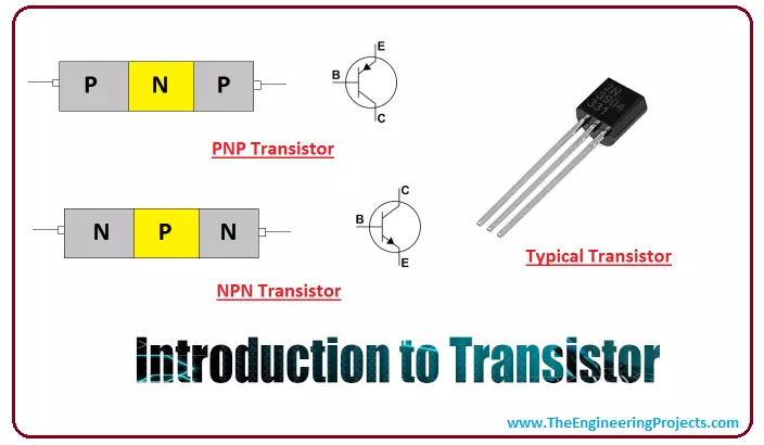
Hi Guys! Hope you are doing fine. Today, I am going to give you a detailed Introduction to Transistor. A transistor is a semiconductor device that comes with three terminals, where a small current at one terminal is used to control current at the other terminals. Transistors are mainly used for the amplification of electronic signals. Transistors were first invented by American Physicists John Bardeen in 1947. Before the inception of transistors, vacuum tubes were used to control the electronic signals. These vacuum tubes come with anode & cathode arrangement and the potential difference across these ends produces the electric current. In the later versions, a filament is added which is used to provide heat to the cathode that directs the electrons towards the anode side. Their complex design, more power consumption set a pathway for the development of the transistors that play an important role in the creation of modern electronic devices. Before you get ahold of the transistor, I'd highly suggest you read the article on which is the building block of the transistor.

What is Diode?

Before going into the details of the transistor, let's first recall some points from the previous lecture Introduction to Diode:
  • A diode is a semiconductor device, that is developed when two types of semiconductor materials(i.e. N-Type and P-Type) are joined together.
  • In the construction of the diode, the PN junction is formed by the combination of P-type & N-type material.
  • Electrons(-ve charge) are major charge carriers in the N-Type material and Holes(+ve charge) are major charge carriers in the P-Type material.
Transistors are formed when an extra layer is added to this PN junction. Transistors come in various types including BJTs, JFETs, MOSFET. BJTs are the bipolar junction transistors which use two charge carriers i.e. electrons and holes for electrical conduction. And BJTs are the current controlled devices where small current at one terminal is used to control large current at other terminals. While JFETs are the unipolar devices where conduction is carried out by the movement of only one charge carrier. Let's dive in and explore what is the main function of a transistor and how it is used for the development of many electronic circuits.

Introduction to Transistor

  • A transistor is a three-terminal electronic device where small current at one terminal is used to control large current at other terminals. Transistors are mainly used for the amplification of the electronic signals.
  • Transistor comes with three terminals called emitter, base, and collector which are used for the external connection with electronic circuits.
  • Transistors were created with the intention of providing cheap electronics. They are available individually, however, most of the time they are packed together in integrated circuits which are then used for the developments of processors, computer memory chips, and complex ICs.
  • A transistor is a combination of two words i.e. transfer and varistor where each layer comes with an ability to transfer current to other layers when a proper biasing voltage is applied across one of the layers.
  • Transistor comes with three layers and two PN junctions where an emitter-base junction is forward biased and the collector-base junction is reverse biased.
  • Most of the transistors are created using silicon and germanium that are less expensive to vacuum tube and require less power to operate.
  • Based on the mobility of major charge carriers, transistors are divided into two types NPN and PNP transistors. Both are different in terms of electrical behaviors and physical construction.
  • The NPN transistors comes with three layers i.e. two N-doped layers and one P-doped layer. The P-doped layer is sandwiched between two N-doped layers. In NPN transistors, conduction is carried out by both charge carriers i.e. electrons and holes, however, electrons are major charge carriers in NPN transistors.
  • Similarly, PNP transistors comes with three layers i.e. two P-doped layers and one N-doped layer. The N-doped layer exists between two P-doped layers. Actually, N-doped layer is responsible for triggering transistor action. When a proper bias voltage is applied at the P-doped layer, it draws current which is then used to control large current at other terminals.
  • Transistors that come in NPN and PNP configurations are nothing but the combinations of two diodes joined back to back.
  • In NPN transistor current flows from collector to emitter, while in PNP transistor current flows from emitter to collector.
  • The current directions and voltage polarities are always opposite in both transistors. Suppose, if a current is flowing in a clockwise direction in NPN transistor and comes with positive polarity at the base terminal, it will flow in an anticlockwise direction in PNP transistor where voltage polarity becomes negative.
  • PN junction formed between two semiconductor material is a building block of the transistor. When PN junction is formed, major charge carriers in N-region (electrons) cross the junction and reach the P-region where they recombine with holes. Similarly, major charge carriers in P-region (holes) cross the junction and reach the N-region where they recombine with electrons.
  • The diffusion of electrons and holes depends on the biasing voltage applied across the junction.
  • The voltage is said to have forward biased when P-region is connected with positive terminal of the battery and N-region is connected with the negative terminal of the battery.
  • Under the forward biased condition, holes and electrons can easily cross the junction and maintain a current across the junction. When this diffusion occurs, it will generate the region across the junction which is depleted with major charge carriers. This region is known as depletion region.
  • As long as the forward biased voltage is applied, current flows across the junction. Diffusion of holes and electrons create an electric field within the junction. This electric field resists the further diffusion of charge carriers.
  • As said earlier, transistor comes with two PN junctions where one junction is forward biased and other junction is reverse biased.

Modes of Transistor

Transistor comes with different modes of operation. Let's discuss them one by one.
Active Mode
  • Active mode is used for amplification of the electronic signal where small current at the base terminal is being amplified at the collector terminal.
  • The base terminal is responsible for the transistor action which controls the number of main charge carriers (electrons in case of NPN transistor and holes in case of PNP transistor) flowing through it and draws a small current when a proper bias voltage is applied.
Cut-Off Mode
  • In this mode, transistor works as an open switch and no current flows across the terminals where a base voltage is less than a voltage at other terminals.
Saturation Mode
  • This mode is considered as an ON switch where current flows freely from collector to emitter.
  • In this condition, the voltage difference between collector and emitter is zero, and the collector current is restricted by a supply voltage and load resistance.
  • In saturation mode, both junctions are forward biased and base voltage is greater than the voltage at other terminals.
Reverse Active Mode
  • This mode acts as an active mode with one exception i.e. current direction is reversed.
  • Current flows from emitter to collector which is proportional to the base current.
  • The base current is highly influenced by the bias voltage applied at the terminal which then controls large current at other terminals.
  • The voltage at the terminals is related in the following way.

Current Gain

Current gain plays an important role in the function of the transistor. Following are two common current gains in a transistor.
Common-Emitter Current Gain
  • Common-Emitter current gain is a ratio between collector current and base current.
  • This is also known as an amplification factor which defines the amount of current being amplified.
  • It is called beta and denoted by ß. The beta value ranges from 20 to 1000, however, most of the time its value is taken as 50.
Common-Base Current Gain
  • Another current gain is common-base current gain which is a ratio between collector current and emitter current.
  • It is called alpha and denoted by a. The alpha value is taken as unity.
Applications of Transistor
  • Transistors are mainly used for the amplification of low and high-frequency AC signals.
  • No current is produced at the collector terminal unless there is a current at the base terminal. This process allows the transistor to work as a switch. The transistor can be turned ON and OFF by controlling the bias voltage at the base terminal.
  • Based on requirements, a transistor can be made to operate in cut-off or saturation region for switching applications.
  • Integrated circuits added in the development of the processors are made from transistors.
  • Used in the development of logarithmic converters and logic gates.
  • Transistors are widely used in modern electronics especially where signal processing and radio transmission is required.
That's all for today. I hope you have found this article useful. We always keep your demands on the top and develop a content that truly resonates with your field of interest. If you are unsure or have any question, you can ask me in the comment section below. I'd love to help you in any way I can. Thanks for reading the article.

What is PN Junction? Forward-Biased | Reverse-Biased

Hey Guys! I hope you all are doing great. In the previous tutorial, we studied the basics of Semiconductors, where we briefly discussed the PN Junction. Today, we are going to have a detailed overview of PN Junction.

But before getting into the details of PN Junction, we need to first recall a few concepts from the previous lecture:

Semiconductor Basics

As we know, the conductive power of a semiconductor material lies between a conductor and an insulator. So, it can act as a pure conductor as well as a pure insulator, depending on the applied conditions.

Semiconductors are divided into two types:

  • Intrinsic Semiconductor.
  • Extrinsic Semiconductor.

Intrinsic Semiconductor

  • A semiconductor in its pure form is called an Intrinsic semiconductor.
  • In this state, the outermost valance shell of the semiconductor has an equal number of electrons and holes(which is 4).
  • These four valance electrons in the outermost shell of an Intrinsic semiconductor remain bound to their positions and thus no conduction is allowed.
  • So, an Intrinsic Semiconductor acts as a pure insulator.
  • The elemental Silicon(Si) or Germanium(Ge) in its pure form is an intrinsic semiconductor.

Extrinsic Semiconductor

  • In order to increase the conductive power of semiconductors, small amounts of impurities(in the ratio of 1 to 106) are added to them, by a method called Doping.
  • Such doped/impure semiconductors are called Extrinsic Semiconductors.
  • Impurities added in the semiconductors are of two types i.e.
    • Pentavalent (Arsenic, Antimony, Phosphorous etc.).
    • Trivalent (Aluminium, Boron, Indium, Gallium etc.)
  • If the semiconductor is doped with a Pentavalent impurity, it's called N-Type Semiconductor.
  • If the doping element used is trivalent, the extrinsic semiconductor produced will be called P-Type Semiconductor.

So, now we need to understand the formation of N-Type and P-type semiconductors, because PN Junction is formed by joining these two types.

N-Type Semiconductors

  • Pure semiconductors normally belong to the 4th column of the periodic table and thus have an equal number of electrons & holes in their valance shell(which is 4).
  • So, in pure form, there's no free electron or hole available for the conduction of electricity and thus it acts as an insulator. (We discussed conduction energy levels in detail in our last lecture)
  • The pentavalent elements belong to the 5th column of the periodic table and have 5 electrons in their outermost shell.
  • So, when a pure semiconductor i.e. Silicon(Si) is doped with a pentavalent impurity i.e. Boron(B), the four valance electrons of the Boron(B) will create a covalent bond with the closest Silicon(Si) atoms, but the 5th electron won't find a pair and will become a free electron.
  • This free electron increases the conductive ability of the semiconductor.
  • As an electron carries a negative charge, such extrinsic semiconductors are called Negative-Type Semiconductors or N-Type Semiconductors.
  • In N-Type Semiconductors, the majority charge carriers are free electrons(negative), while the holes(positive) are present in very small numbers(called minority charge carriers).

Now let's have a look at the formation of P-Type Semiconductors:

P-Type Semiconductors

  • When a semiconductor is doped with a trivalent impurity i.e. Aluminium(Al), the extrinsic semiconductor produced is called P-Type Semiconductor and has positively charged holes as majority charge carriers.
  • Trivalent elements belong to the 3rd column of the periodic table and have 3 electrons in their outermost shell(valence shell).
  • So, if we dope Silicon(Si) with Aluminium(Al), the 3 valence electrons of the impurity element(Al) will create a covalent bond with the neighboring Silicon(Si) atoms.
  • The 4th valence electron of Si won't find a pair and thus a positively charged Hole will be originated. A Hole is a vacant space, has a positive charge and is ready to accommodate an electron(if available).
  • This Hole generated in the Si crystal will increase its conductivity and such doped semiconductor will be called Postive-Type Semiconductor or P-Type Semiconductor.

So far, we have created N-Type and P-Type Semiconductors by adding pentavalent and trivalent impurities respectively in separate semiconductor crystals. Now, we are going to add both impurities in a single semiconductor crystal to create a PN Junction. So let's get started:

What is PN Junction?

  • When a single crystal of semiconductor is doped with both pentavalent(i.e. Boron) and trivalent(i.e. Aluminium) impurities, a special barrier is created at the boundary of the two regions(N-Type & P-Type) which stops the flow of charge carriers. This barrier is called PN Junction.
  • The most basic semiconductor component called Diode is a real-life application of the PN Junction.

Now let's have a look at the formation of this PN Junction:

PN Junction Formation

  • As we know, electrons are the majority charge carriers in N-Type Semiconductors and Holes are the majority charge carriers in P-Type Semiconductors.
  • Now, when we dope a single Si crystal with both impurities, an N-Typer region is created on one side and a P-Type region is created on the other side of the crystal.
  • Electrons(in the N-Type region) present near the boundary get excited and diffuse into the P-Type region. Similarly, the Holes(in the P-Type region) close to the boundary move towards the N-Type region.
  • This generates a potential difference at the boundary of the two regions, which gradually increases and at one point, restricts the further flow of electrons or holes in the neighboring region. (electron-hole diffusion stops)
  • This region at the boundary with electrons in the P-Type region and Holes in the N-Type region is called the depletion region.
  • The width of this depletion region depends on the amount of impurity added to the semiconductor.
  • This Junction/boundary of the P-Type and N-Type regions is called the PN Junction.
  • Under normal conduction, when there is no voltage applied across the PN junction, the junction is said to be in an equilibrium state. The potential difference at the junction in that state is called built-in potential which is 0.7 V for Silicon(Si) and 0.3 V for Germanium(Ge).
  • When an external voltage is applied at the PN Junction, we get two behaviors of PN Junction depending on the external voltage polarity, named:
    1. Forward-Biased.
    2. Reverse-Biased.

Let's discuss these diode states, one by one:

Forward-Biased PN Junction

  • If the positive terminal of the battery is connected to the P-region and the negative terminal to the N-region, the PN Junction will be said to be operating in a Forward-Biased State.
  • The external voltage should be greater than the built-in potential i.e. 0.7V for Si and 0.3V, so that it could melt the depletion region.
  • In the Forward-Biased State, the Holes start to move towards the N-region and the electrons start flowing towards the P-region.
  • As a result, the width of the depletion region starts reducing and finally depletes out.
  • The current starts flowing through the semiconductor, as soon as the depletion region gets removed. We can say the semiconductor is acting as a conductor.
  • In this state, the semiconductor has maximum conductivity and quite low resistance.

Reverse-Biased PN Junction

  • If the P-region is connected with the negative terminal of the external source and the N-region with the positive terminal, the PN-Junction will operate in the reverse-biased state.
  • As the P-region is connected to the negative voltage, the holes in the P-region will get attracted towards the external voltage, so start flowing away from the depletion region. The same will be the case with the electrons.
  • So, no current will flow through the PN Junction in a reverse-biased state.

PN Junction as a One-Way Switch

In a normal conductive wire, current can flow in both directions but in a PN Junction, the current will flow only in one direction and will get blocked in the opposite direction. So, we can say that a PN-Junction is a One-Way Switch, allowing the current to flow in one direction only. On the top of my head, it could be used to avoid the back emf generated by the motors. This One-way switch literally bought a revolution in electronics.

Breakdown Region

  • While the PN Junction is operating in the reverse-biased state, if the external voltage exceeds a certain limit, the PN Junction will collapse, resulting in an excessive amount of current flow(short-circuit). This external voltage is called breakdown voltage and the PN Junction is said to be operating in a breakdown region.
  • PN Junction can't recover from the breakdown region so it should be avoided, though it also has a few advantages, which we will cover in the Zener Diode Chapter.
  • The breakdown voltage depends on the semiconductor used and the amount of impurity added.

Characteristic Curve of PN Junction

The following figure shows the I vs V characteristic curve of a silicon diode:

  • As we can see in the above characteristic curve of PN Junction, it has two sections i.e. forward-biased and reverse-biased.
  • In the forward-biased state, if the voltage is lower than the built-in potential(i.e. 0.7 for Si), a small amount of current is flowing through the PN Junction but if the voltage overcomes the built-in potential, the current jumps to its maximum value and we can say the PN Junction is conducting.
  • In the reverse-biased state, there's no current flowing through the PN Junction until the breakdown voltage is reached.
  • At the breakdown voltage, the current starts flowing in the opposite direction and we can say the PN Junction collapsed.
  • The small current flowing under reverse bias normal condition is known as leakage current. Germanium(Ge) has more leakage current as compared to Silicon(Si).

So, that's all for today. I hope you have enjoyed today's lecture. In the next lecture, we will discuss the Basics of Diodes, where I am going to repeat today's lecture :)) But I will keep the practical approach in it, so there will be a lot to learn. If you have any questions, you can approach me in the comment section below. Keep your suggestions and feedback coming, they help us deliver quality content. Thanks for reading the article.

Syed Zain Nasir

I am Syed Zain Nasir, the founder of <a href=https://www.TheEngineeringProjects.com/>The Engineering Projects</a> (TEP). I am a programmer since 2009 before that I just search things, make small projects and now I am sharing my knowledge through this platform.I also work as a freelancer and did many projects related to programming and electrical circuitry. <a href=https://plus.google.com/+SyedZainNasir/>My Google Profile+</a>

Share
Published by
Syed Zain Nasir