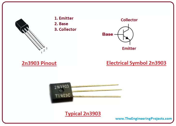
Introduction to PNP Transistor


Introduction to PNP Transistor
- The PNP transistor is a type of bipolar transistor used for amplification and switching purpose and for the designing of the complementary output stage in combination with NPN transistor.
- It comes with three terminals called emitter, base, and collector where small current at the base terminal is used to control large current at other terminals.
- It is a current controlled device also known as sinking device where it sinks current into its base terminal and current flows out of the collector.
- Unlike NPN transistor, current flows from the emitter to collector in this PNP transistor and holes act as a majority charge carriers.
- This transistor comes with same characteristics as NPN transistor but there are some exceptions. In case of PNP transistor, all voltage polarities and current directions will be reversed as compared to NPN transistor. The PNP transistor sinks current into its base while NPN transistor sources current through its base terminal.
- Both NPN and PNP transistors are current controlled devices where conduction is carried out by both charge carriers i.e. electrons and holes, but major charge carriers are electrons in case of NPN transistors. While in case of PNP transistor major charge carriers are holes.
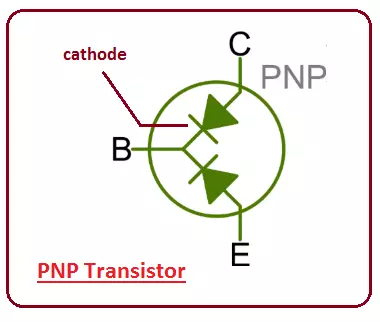
- The PNP transistor is like a combination of diodes combined back to back from cathode sides.
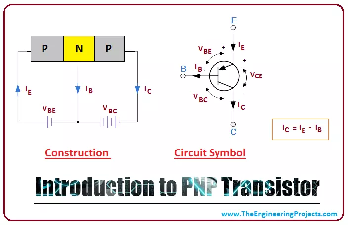
Construction
- This PNP transistor is composed of two P-doped layers and one N-doped layer where N-doped layer represents the base of the transistor while other P doped layers represent emitter and collector respectively.
- The base of the transistor is more negative than the emitter terminal.
- All three terminals in the PNP transistor are different in terms of doping concentration and size.
- An emitter is highly doped and exhibits 100% current of the transistor while a base is lightly doped which is responsible for the transistor action and controls the number of holes in case of PNP transistor.
- While collector is lightly doped and comes in a bigger size as compared to other two terminals and collects the number of holes.
Circuit Diagram
- Following figure shows the circuit diagram of PNP transistor.
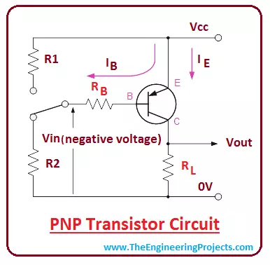
- In PNP transistor, a source voltage is applied at the emitter terminal (instead of collector terminal in case of NPN transistor) and load resistor is applied that is used to resist the current in the collector terminal.
- Similarly, a bias voltage is applied at the base terminals and a base resistor is connected to this terminal in order to limit the current flowing through this terminal.
- The emitter is connected to a positive voltage while the base is connected to the negative voltage.
Working
- Similar to NPN transistor, PNP transistor comes with two pn junctions i.e. emitter-base junction and collector-base junction.
- An emitter-base junction is forward biased and shows low resistance while collector-base junction is reverse biased and exhibits high resistance. Steps and process required to make these junctions forward biased and reverse biased are different than NPN transistors.
- Emitter-base junction will become forward biased when a base is negative with respect to the emitter and the voltage at the base side is 0.7 V less than the voltage at the emitter side.
- Similarly, emitter-base junction is made reverse biased when applied collector voltage is negative. In case of PNP transistor, emitter voltage is much larger than collector voltage.
- In order to conduct for PNP transistor, emitter voltage must be more positive as compared to both base and collector.
- The transistor will turn on when there is small current flowing from emitter to base terminal.
- In PNP transistors emitter emits holes as compared to NPN where emitter emits electrons.
- When a proper bias voltage is applied at the base terminal, it gets biased and the holes present at emitter terminal moves to the base terminal where they combine with the electron present at this terminal. This generates the small current at the base terminal.
- The base is very thin so it is very difficult for a base to accept all holes injected by the emitter, as a result, most of the holes leave the base terminal and enter collector terminal.
Matched Switch
- Combination of PNP transistor with NPN transistor is used for designing and development of the power amplifier circuits. Power B amplifiers are the great example of this amplifier circuits where both PNP and NPN transistors are incorporated together to generate high amplification cycle.
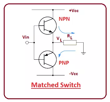
- Pair of NPN and PNP transistor used in Class B amplifiers is called complementary or matched switch where PNP transistor conducts for the negative half cycle while NPN transistor conducts for the positive half cycle of the transistor.
- This process is used to generate required power for the loudspeaker in both directions. The resulting power generates at the output current is very high which is then equally shared between matched switch composed of NPN and PNP transistor.
Output Characteristics Curve
- The output characteristic curve of PNP transistor looks identical to that of NPN transistor but there is one exception i.e. it is rotated by 180 degrees.
- The same load line is drawn on the characteristic curve that we drew in case of NPN transistor that mentions the operating points of the transistor.
- The following figure shows the characteristics curve of PNP transistor which is drawn between the output current and collector-emitter voltage and is rotated by 180 degrees where current directions and voltage polarities are reversed. The supply voltage becomes negative for PNP transistor.
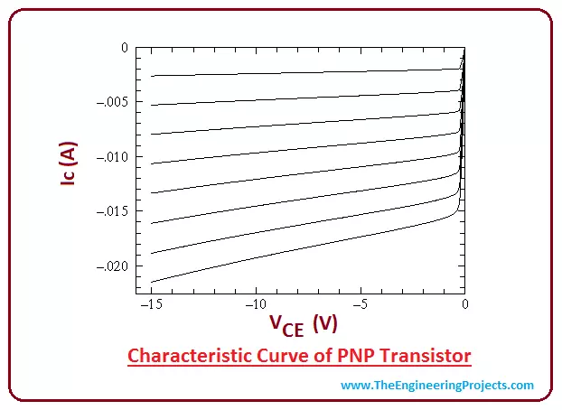
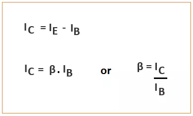
- The current gains (alpha, beta) value are much less in PNP transistor as compared to NPN transistor. We can calculate the beta value from the following equation;
Difference between PNP and NPN Transistors
- The PNP transistor is known as sinking device while NPN transistor is known as sourcing device.
- The main difference between PNP and NPN transistor is the proper biasing of the base terminal where current directions and voltage polarities are always opposite to each other.
- In PNP transistor, holes are majority carriers while in NPN transistor electrons are majority carriers.
- The emitter voltage is made more positive as compared to both base and collector in PNP transistor. While collector voltage is made more positive as compared to base and emitter in case of NPN transistor.
- The PNP transistor will be considered ON when there is no current at the base terminal. The NPN transistor will be considered ON when there is enough current present at the base terminal.
- In PNP transistor current flows from the emitter to collector, while in case of NPN transistor current flows from collector to emitter.
- The base is positive in case of NPN transistor while it is negative in PNP transistor.
- When there is enough voltage applied at the base terminal it gets biased in case of NPN terminal while in case of PNP transistor, negative voltage 0.7 V less than emitter voltage must be applied to trigger transistor action.
Applications
- This transistor is used as a switch for electronic signals.
- It is used in amplifying circuits.
- Used as a matched switch in combination with NPN transistor for generating continuous power.
- Current flow involving heavy motors makes use of these transistors.
- Used in robotic applications where current sinking is required.
×
![]()