


Introduction to 2n3903


Introduction to 2n3903
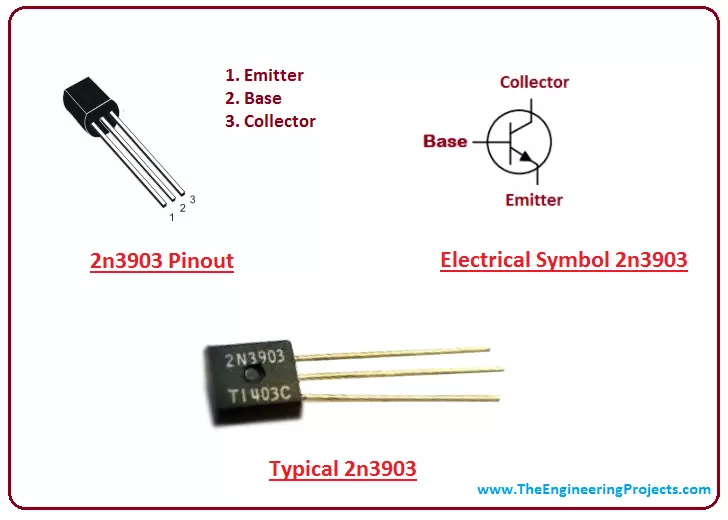
- The 2n3903 is an electronic component called NPN transistor mainly used for general purpose amplification and switching applications.
- It comes with three terminals called emitter, base, and collector.
- This transistor has three layers i.e. two N-doped layers and one P-doped layer. The P-doped layer is a semiconductor that is housed between two N-doped layers.
- The P-doped layer represents the base of the transistor while other two layers represent emitter and collector respectively.
- All three terminals are different in terms of their size and doping concentration. The emitter is highly doped as compared to base and collector.
- The base is lightly doped which is responsible for the electron reaction when a voltage is applied at this terminal. When a voltage is applied, it draws small current which is then used to control large current at the emitter and collector terminals.
- Under normal conditions, the number of electrons diffused into the base terminal is more than the number of holes diffused into the emitter terminal. Electrons act as a majority charge carriers in case of NPN transistor.
- This transistor is an ideal choice for amplification and switching purpose requiring collector current around 100mA.
Pinout of 2n3903
Following figure shows the pinout of this NPN transistor which is composed of three terminals. 1. Emitter 2. Base 3. Collector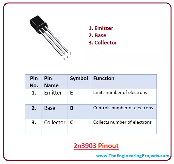
- Movement of electrons plays an important role in the current flowing from emitter to collector.
- The output current obtained at the output terminals is highly dependent on the voltage applied to the base terminal.
- This bipolar transistor is a current controlled device where small current at the base terminal is used to control large current at other terminals. It is different than MOSFET that is voltage controlled unipolar device where conduction is carried out by one charge carrier i.e either electron or hole.
Circuit Diagram of 2n3903
- Following figure shows the circuit diagram of this NPN transistor.
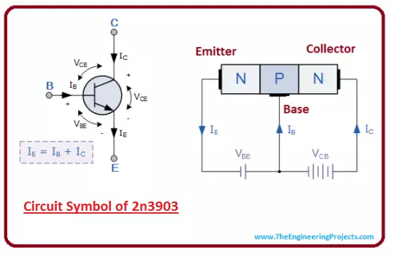
- The emitter is highly doped so it exhibits more current as compared to other terminals. Actually, current at the emitter terminal is a sum of the current at the base and collector terminal.
- Common-Emitter current gain plays an important role in the amplification process. It is a ratio between collector current and base current. It is called beta and denoted by ß. This is also called amplification factor which defines the amount of current being amplified.
- Common-Base current gain is another important factor which exhibits lower value than beta. It is a ratio between collector current and emitter current. It is called alpha and denoted by a. Alpha value ranges between 0.95 to 0.99 and most of the time its value is taken as unity.
Absolute Maximum Ratings of 2n3903
- Following figure shows the absolute maximum ratings of this NPN transistor.
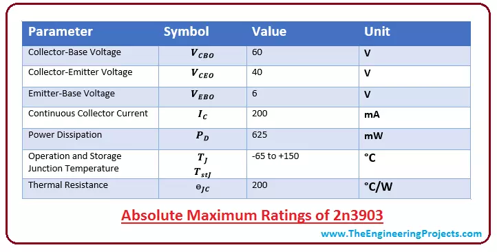
- These are the stress ratings which play an important role in the execution of the electronic circuit. If these stress ratings are exceeded from absolute maximum ratings, they can damage the device at large, ultimately affecting the overall nature and performance of the project.
- Similarly, if these ratings are applied for the maximum period of time above normal operating conditions they can affect the reliability of the device.
- It is advised to check these ratings before placing the device in the circuit and make sure device undergoes and follows same operating conditions and stress ratings as defined by the manufacturer.
- Steps and measurements taken in the early stages of your project can save you bunch of time and worry and prevents electronic circuit from being affected.
Difference between PNP and NPN Transistors
- NPN and PNP work in a similar way with the intention of amplification and switching purpose but there is some difference between them.
- Voltage polarities and direction of currents are opposite in these transistors.
- Electrons are majority charge carriers in case of NPN transistors while holes are majority charge carriers in case of PNP transistors, however, both types of transistors require both charge carriers for complete conduction process.
- The base is negative in case of PNP transistor and a negative voltage is applied at the base terminal in order to trigger the holes reaction. And the base is more negative as compared to emitter and collector.
- While in case of NPN transistor, a base is positive and positive voltage is applied at this terminal in order to trigger electron reaction which draws small current that is used to control large current at the emitter and collector terminals.
- These transistors are nothing but a combination of diodes joining back to back.
Applications
- This transistor is mainly used for amplification and switching purpose where collector current around 100mA is required.
×
![]()


