


Introduction to 2n5551


Introduction to 2n5551
- 2n5551 is an NPN bipolar junction transistor which is mainly used for general purpose amplification and gas discharge display drivers.
- It consists of three terminals known as the emitter, base, and collector and comes in a TO-92 package.
- Unlike FETs, this NPN transistor is a current controlled device where small current at the base side is used to control large current at the emitter and collector side.
- As it is an NPN transistor so the base will be positive with respect to the emitter.
- It features high breakdown voltage, low leakage current, capacity and beta value which are very useful over a wide range of current.
- Movement of electron plays an important role in defining the conducting nature of any transistor. This NPN transistor is known as BJT (bipolar junction transistor) because conduction is carried out by both electrons and holes but majority charge carriers are electrons.
- Whenever a voltage is applied at the base, it gets biased and controls the current at the emitter and collector side.
- The emitter emits the electrons which are collected by the collector. A base is used to control the number of electrons.
- The ability of the base to control the number of electrons is used for amplification purpose.
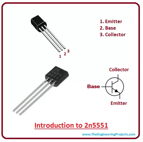
2n5551 Pinout
2n5551 is an NPN transistor, also known as a current controlled device which contains three terminals as follow. 1. Emitter 2. Base 3. Collector
- It is different than JFET which is a unipolar transistor, also known as a voltage controlled device.
- Transistor action is triggered when a voltage is applied at the base side which allows the free movement of electrons.
- Movement of free electrons is nothing but a bridge between emitter and collector.
Circuit Diagram of 2n5551
The circuit diagram of 2n5551 is shown in the figure below.
- The emitter current is equal to the sum of collector and base current.
- The voltage at the base side must be positive with respect to the emitter for current flow from emitter to collector.
- Forward current gain is an important factor in determining the characteristics of this transistor. It is called Beta and represented by ß. It is a ratio between collector current to the base current. As it is a ratio between two current so it exhibits no unit.
- Beta value is also known as amplification factor which determines the value of current being amplified.
- Beta value ranges between 20 to 1000 but it comes with a standard value of 200.
- The current gain of the transistor is another important factor which is called alpha and represented by a. It is a ratio between collector current and emitter current. Alpha value ranges between 0.95 to 0.99 but most of the time its value is taken as unity.
- The NPN transistor mainly consists of two diodes combined back to back.
Absolute Maximum Ratings
Following figure shows the absolute maximum ratings of 2n5551.
- Collector-Emitter and Collector-Base voltages are 160 and 180 respectively.
- And maximum power it can dissipate is 630 mW.
- These are the stress ratings which if exceeded from absolute maximum ratings, can damage the device at large.
- Similarly, if stresses are applied for an extended period of time, they can affect the overall reliability of the device.
Difference between NPN and PNP Transistors
- The main difference between these two transistors is the type of charge carrier.
- Electrons are main charge carriers in case of NPN transistors while holes are main charge carriers in case of PNP transistors.
- Most of the experts prefer NPN transistors for most of the applications because they consider conduction through electrons is better than conduction through holes.
Applications
- 2n5551 comes with high breakdown voltage and is mainly used in gas discharge display drivers.
- General purpose amplification is another feature of this NPN transistor which makes it an ideal choice for most of the professionals.
×
![]()


