Introduction to 2n5401

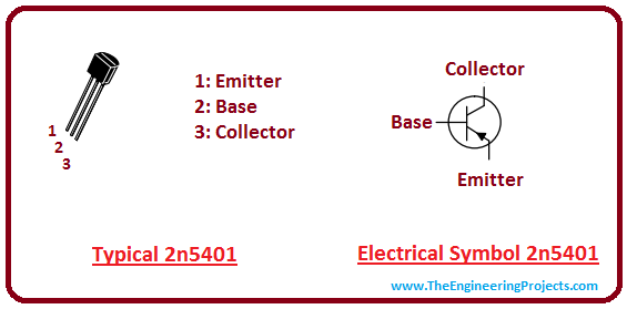
Introduction to 2n5401
- 2n5401 is a PNP bipolar junction transistor, also known as amplifier transistor, that comes with collector-emitter voltage of 150V and mostly used for amplification purpose.
- In order to operate this transistor properly in the circuit, no external components are required.
- Most of the professionals prefer this device over common resistor/zener approach.
- It exhibits current limiting and thermal shutdown which make the device substantially rugged.
- It consists of three terminals named as emitter, base and collectors.
- Small current at the base side is used to control the large current at the emitter and collector side.
- It is a bipolar junction transistor where conduction is carried out by both electrons and holes but majority charge carriers are holes.
- As it a PNP transistor so P side represents the polarity at the emitter side which is positive and N represents the polarity at the base side which is negative.
- Base will always be negative will respect to emitter.
2n5401 Pinout
2n5401 is a PNP transistor which mainly consists of three terminals.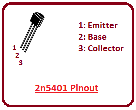
- Conduction is carried out from emitter to collector and majority charge carriers will be holes rather than electrons.
- Transistor works in a way, it allows small current at the base side to control large current at the emitter or collector side.
2n5401 Circuit Diagram
Circuit symbol of 2n5401 is shown in the figure below.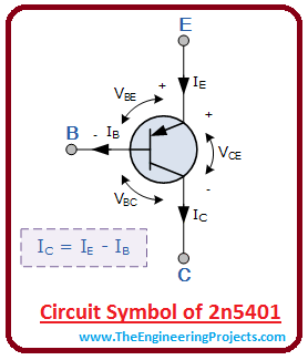
- Emitter polarity will be positive as compared to base and collector.
- Conduction is carried out when base will be negative as compared to emitter.
- Emitter current is the sum of current at the base and collector side.
- PNP works in a similar way like NPN transistors with some exceptions. In PNP transistors, directions of current and voltage polarity will be reversed and majority charge carriers will be holes.
- Some professionals NPN transistors over PNP transistors, because conduction through mobility of electrons is better than conduction through mobility of holes.
Absolute Maximum Ratings of 2n5401
Following shows the absolute maximum ratings of 2n5401.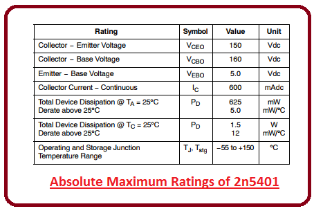
- Collector-Emitter voltage and Collector-Base voltages are 150 and 160 V respectively.
- Total power dissipation at the collector side is 625 mW.
- These are the stress rating. If stresses are exceeded from given absolute maximum ratings, they can damage the device.
- Similarly, if stresses are applied for extended period of time, they can effect the device reliability.
Transistors as a Matched Switch
- PNP transistors widely replace NPN transistors in some applications because both exhibit same properties with some exception i.e. direction of current and polarities of voltage will be reversed.
- Both PNP and NPN transistor can be used for switching applications.
- PNP and NPN transistors can be incorporated in a same circuit to design the power amplifier circuits.
- Class-B amplifiers are incorporated with two pairs of PNP and NPN transistors where both transistors are used to control the current flowing in both directions.
- Transistors are termed as "Complementary Transistors" which use both pair of PNP and NPN transistors.
- Both NPN and PNP transistors work in a similar fashion i.e. PNP conducts for the negative half cycle of the transistor while NPN conducts for the positive half cycle of the transistor. This process helps in flowing the power at the load output in both directions.
- Main difference between PNP and NPN transistor is that current will sink to its base side in case of PNP transistor while current will source from base to the transistor in case of NPN transistor.
Applications
- It is mainly used for general purpose amplification and switching purpose.
- Telephony applications involve these NPN transistors.
- These transistors cannot be used in life support appliances because any defect in these transistors can cause the personal injury.
×
![]()


