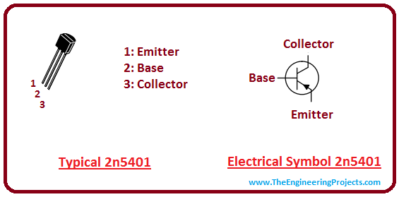
Introduction to 2sa1015

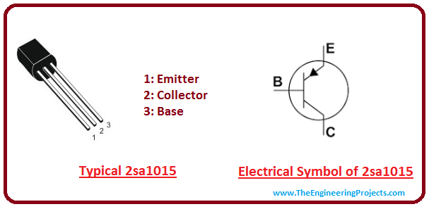
Introduction to 2sa1015
- 2sa1015 is a PNP low frequency transistor which is mainly used for general purpose amplification.
- It mainly consists of three terminals called emitter, base and collector.
- N layer of this transistor represents the base side while other two P layers represent emitter and collector receptively.
- Base is always negative with respect to emitter.
- As it is bipolar junction transistor so conduction is carried out by both charge carriers i.e. electrons and holes, but majority charge carriers will be holes.
- When negative voltage is applied at the base side it gets biased and current starts to flow from emitter to collector.
- It is referred as a current control device because small current at the base side is used to control the large current at the emitter and collector side.
- In this PNP transistors P layer shows the polarity applied at the emitter side which is positive while N side shows the polarity at the base side which is negative.
- Current will only flow when base is negative with respect to emitter.
2sa1015 Pinout
This PNP transistor mainly consists of three terminals.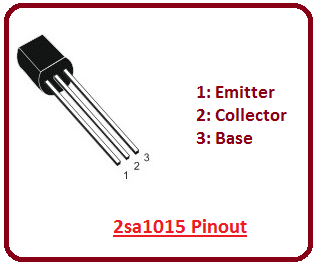
- Base side is lightly doped while emitter side is heavily doped.
- Difference between emitter and collector is their size and doping concentration. Emitter is heavily doped while collector is lightly doped.
Circuit Diagram of 2sa1015
Following figure shows the circuit diagram of 2sa1015 PNP transistor.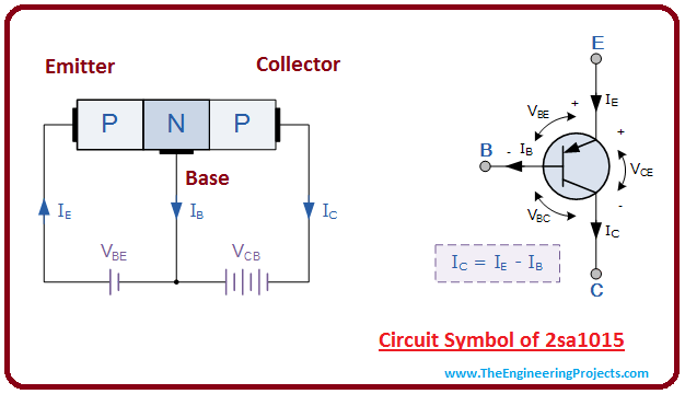
- Current at the emitter side is the sum of current at base and collector side.
- Current will flow from collector to emitter and majority charge carriers will be holes.
- This transistor is referred as a current controlled device where small current at the base side is used to control large current at the emitter and collector side.
Absolute Maximum Ratings of 2sa1015
Following figure shows the absolute maximum ratings of 2sa1015.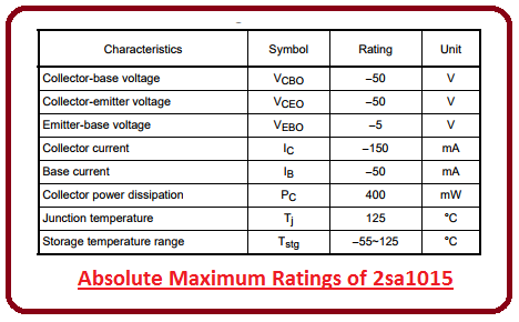
- Collector-Base and Collector-Emitter voltage is -50.
- And maximum collector power dissipation is 400 mW.
- These are the stress rating above which device can damage.
- If stresses are applied for extended period of time, they can effect the device reliability.
Difference between PNP and NPN Transistors
- Both NPN and PNP works in a similar way with some exceptions. Voltage polarity and current directions will be reversed in case of PNP transistors as compared to NPN transistors.
- In case of PNP transistor, current will sink to its base side while in case of NPN transistor, base sources current to the transistor.
- Most of the professionals prefer NPN transistor over PNP transistors because they consider conduction through mobility of electrons is better than conduction through mobility of holes.
Transistors as a Matched Switch
- Both NPN and PNP transistors behave like a switching devices.
- You might come across an idea what is the purpose of using PNP transistors while there are already tons of NPN transistors out there which can be used for amplification. However, when PNP transistors are used in combination with NPN transistors, they help in designing the perfect power amplifier circuit.
- Class B amplifiers widely use combination of both NPN and PNP transistors where both transistors are used to control the current flowing in both directions at any time.
- Transistors are called complementary transistors which use both NPN and PNP transistors of same characteristics.
- In Class B-amplifiers, both NPN and PNP transistors work in a same fashion i.e. NPN transistors conducts for the positive half cycle and PNP transistor conducts for the negative half cycle of the transistor. This results in flowing the power at the load output in both directions.
Applications
- These transistors are widely used for voltage and power amplification.
- When these transistors are incorporated with NPN transistors, they construct a perfect bond and current starts to flow from both sides of NPN and PNP transistors.
×
![]()


