Introduction to ATmega328

Hello everyone! I hope you all will be absolutely fine and having fun. Today, I am going to give you a detailed Introduction to ATmega328. ATmega328 is an Advanced Virtual RISC (AVR) microcontroller. It supports 8-bit data processing. ATmega-328 has 32KB internal flash memory.

ATmega328 has 1KB Electrically Erasable Programmable Read-Only Memory (EEPROM). This property shows if the electric supply supplied to the micro-controller is removed, even then it can store the data and can provide results after providing it with the electric supply. Moreover, ATmega-328 has 2KB Static Random Access Memory (SRAM). Other characteristics will be explained later. ATmega 328 has several different features which make it the most popular device in today's market. These features consist of advanced RISC architecture, good performance, low power consumption, real timer counter having separate oscillator, 6 PWM pins, programmable Serial USART, programming lock for software security, throughput up to 20 MIPS etc. Further details about ATmega 328 will be given later in this section.

Note:
  • Here's the link to download the Atmega328 datasheet, although after reading this article you won't need it. :)
  • Moreover, I have also given the link to a reliable online source from where you can buy it easily.
Download Atmega328P Datasheet
Where To Buy?
No.ComponentsDistributorLink To Buy
1Arduino UnoAmazonBuy Now

Introduction to ATmega328

  • ATmega328 is an 8-bit, 28-Pin AVR Microcontroller, manufactured by Microchip, follows RISC Architecture and has a flash-type program memory of 32KB.
  • Atmega328 is the microcontroller, used in basic Arduino boards i.e Arduino UNO, Arduino Pro Mini and Arduino Nano.
  • It has an EEPROM memory of 1KB and its SRAM memory is 2KB.
  • It has 8 Pins for ADC operations, which all combine to form PortA ( PA0 - PA7 ).
  • It also has 3 built-in Timers, two of them are 8 Bit timers while the third one is 16-Bit Timer.
  • You must have heard of Arduino UNO, UNO is based on atmega328 Microcontroller. It's UNO's heart. :)
  • It operates ranging from 3.3V to 5.5V but normally we use 5V as a standard.
  • Its excellent features include cost-efficiency, low power dissipation, programming lock for security purposes, real timer counter with separate oscillator.
  • It's normally used in Embedded Systems applications. You should have a look at these Real Life Examples of Embedded Systems, we can design all of them using this Microcontroller.
  • The following table shows the complete features of ATmega328:
ATmega328 Features
No. of Pins 28
CPU RISC 8-Bit AVR
Operating Voltage 1.8 to 5.5 V
Program Memory 32KB
Program Memory Type Flash
SRAM 2048 Bytes
EEPROM 1024 Bytes
ADC 10-Bit
Number of ADC Channels 8
PWM Pins 6
Comparator 1
Packages (4) 8-pin PDIP 32-lead TQFP 28-pad QFN/MLF 32-pad QFN/MLF
Oscillator up to 20 MHz
Timer (3) 8-Bit x 2 & 16-Bit x 1
Enhanced Power-on Reset Yes
Power Up Timer Yes
I/O Pins 23
Manufacturer Microchip
SPI Yes
I2C Yes
Watchdog Timer Yes
Brownout detect (BOD) Yes
Reset Yes
USI (Universal Serial Interface) Yes
Minimum Operating Temperature -40 C to +85 C

ATmega328 Pins

  • ATmega-328 is an AVR Microcontroller having twenty-eight (28) pins in total.
  • All of the pins in chronological order, are listed in the table shown in the figure given below.
Now let's have a look at the pinout of Atmega328 in detail:

ATmega328 Pinout

  • Through the pinout diagram, we can understand the configurations of the pins of any electronic device, so you are working on any Engineering Project then you must first read the components' pinout.
  • ATmega328 pinout diagram is shown in the figure given below:

ATmega328 Pins Description

  • Functions associated with the pins must be known in order to use the device appropriately.
  • ATmega-328 pins are divided into different ports which are given in detail below.
  • VCC is a digital voltage supply.
  • AVCC is a supply voltage pin for analog to digital converter.
  • GND denotes Ground and it has a 0V.
    • Port A consists of the pins from PA0 to PA7. These pins serve as an analog input to analog to digital converters. If analog to digital converter is not used, port acts as an eight (8) bit bidirectional input/output port.
    • Port B consists of the pins from PB0 to PB7. This port is an 8 bit bidirectional port having an internal pull-up resistor.
    • Port C consists of the pins from PC0 to PC7. The output buffers of port C has symmetrical drive characteristics with source capability as well high sink.
    • Port D consists of the pins from PD0 to PD7. It is also an 8 bit input/output port having an internal pull-up resistor.
  • All of the AVR ports are shown in the figure given below.
  • AREF is an analog reference pin for analog to digital converter.
  • So this was the brief of all the pins in the ATmega328 AVR micro-controller.

ATmega328 Architecture

  • An architecture of a device presents information about the particular device.
  • ATmega-328 architecture is shown in the figure given below.

ATmega328 Memory

  • ATmega 328 has three types of memories, named:
    • Flash Memory: 32KB. It is a Programmable Read-Only Memory (ROM). It is a nonvolatile memory.
    • SRAM: 2KB. Stands for Static Random Access Memory. It is a volatile memory i.e. data will be removed after removing the power supply.
    • EEPROM: 1KB. Stands for Electrically Erasable Programmable Read-Only Memory.
  • AVR memory spaces are shown in the figure given below.

ATmega328 Registers

  • ATmega-328 has thirty-two (32) General Purpose (GP) registers.
  • These all of the registers are part of Static Random Access Memory (SRAM).
  • All the registers are given in the figure shown below.

ATmega328 Packages

  • The different versions of the same device are denoted by the different packages of that device.
  • Each package has different dimensions, in order to differentiate easily.
  • ATmega 328 packages are given in the table shown in the figure given below.

ATmega328 Block Diagram

  • The Block diagram shows the internal circuitry and the flow of the program of any device.
  • ATmega 328 block diagram is shown in the figure given below.

ATmega328 Features

  • To perform any task we can select a device on the basis of its features. i.e whether its features match to obtain the desired results or not.
  • Some of the main features of an AVR Microcontroller ATmega328 are shown in the table given in the figure below.

ATmega328 and Arduino

  • ATmega328 is the microcontroller used in the Arduino UNO board.
  • When we upload code in Arduino UNO, it's actually uploaded in the Atmega328 Microcontroller.
  • A software driver called bootloader is pre-installed in the flash memory of the Atmega328 microcontroller, which makes it compatible with Arduino IDE.
  • AVR Atmega328 attached on Arduino is shown in the figure given below:

ATmega328 and Arduino Pins

  • ATmega328 pins are connected to the corresponding pins of Arduino.
  • Their connectivity with each other is shown in the pinout diagram shown in the figure given below.
  • The encircled section analog pins consist of the Arduino pins which are connected to the corresponding AVR micro-controller ATmega-328 pins.
  • I have written both of the pins in front of each other, it will help to understand easily.
  • If you want to work on this Arduino board then you must try these Arduino Projects for Beginners, they will help to get your hands on Arduino.

Applications of Atmega328

  • A complete package including ATmega 328 and Arduino can be used in several different real-life applications.
  • It can be used in Embedded Systems Projects.
  • It can also be used in robotics.
  • Quad-copter and even small aero-plane can also be designed through it.
  • Power monitoring and management systems can also be prepared using this device.
  • I have designed this Home Security System using Arduino UNO, you should have a look at it.

How to start working on Atmega328

  • If you want to start working on this Microcontroller then I would suggest you do it using Arduino.
  • The benefit of using Arduino is that you get to use all of its built-in libraries, which will make the work a lot easier.
  • After designing your project on Arduino, then design the basic circuit of Atmega-328 which is quite simple and I have discussed above.
  • Now you must be careful while using its Pins, Atmega328 and Arduino Pins are discussed above.
  • Another thing to mention here is that before working on hardware, you should first design its Proteus Simulation.
  • Download Arduino Library for Proteus and then design your project on it.
  • Once you are confirmed that everything's correct then design its circuitry on Wero Board or PCB (Printed Circuit Board) and you have your project ready. :)
The tutorial Introduction to ATmega328 has the presented a detailed discussion on the basic use of ATmega 328. I have completely provided the entire necessary details about the use of an AVR micro-controller. If you have any problems, you can ask us in the comments anytime. Our team is always here to help you guys. I will share other amazing topics with all of you in my upcoming tutorials. So, till then take care :)

Introduction to LM335

Hello everyone! I hope you all will be absolutely fine and having fun. Today, I am going to share my knowledge about Introduction to LM335. LM 335 is basically an Integrated Circuit (IC) for precise temperature sensor. LM-335 operates on a current range 400uA-5mA having resistance less than 1 ohm. At 10mV/K, its absolute temperature becomes directly proportional to the breakdown voltage. LM-335 operates as two terminal zener diode. At the temperature ranging from -40 degree Celsius to 100 degree Celsius, LM 335 can be used for each type of temperature sensing purposes. This device is available in different dimensions and in different sizes. LM-335 is most commonly available in the market due to its unique features including e.g. large temperature range, cost effectiveness, low dynamic resistance, initial accuracy up to 1 degree Celsius. LM-335 can be used at several different places. Its applications include Heat Ventilation and Air Conditioning (HVAC), power supplies, battery management systems, home appliances, embedded systems etc. The further detail about LM-335 will be given later in this tutorial. [otw_is sidebar=otw-sidebar-7]

Introduction to LM335

LM335 is a low cost temperature sensor and gives highly precised results. It operates as a two terminal zener diode. It has low dynamic impedance less than 1 ohms. It has a large range for temperature i.e. -40 degree Celsius to 100 degree Celsius. At 10mV/K its breakdown voltage becomes directly proportional to its absolute temperature. large temperature ranges, initial accuracy up to 1 degree Celsius and low dynamic impedance are its major and unique features. It can be used in HVAC, home appliances, power supplies etc. LM-335 is shown in the figure given below.
1. LM335 Pins
  • LM 335 has total three (3) pins made up of steel, at the bottom side of the structure.
  • Its pins are listed in the table shown in the figure below.
2. LM335 Pins Description
  • Each pin has carries functions.
  • LM-355 pins along with its description are listed in the figure below.
3. LM335 Pinout
  • Pinout diagram basically helps us to understand the pin configurations of any device.
  • LM 335 pinout diagram is shown in the figure below.
4. LM335 Pins
  • DIfferent packages of a device shows its different versions.
  • LM 335 has three different packages, shown in the table given below.
5. LM335 Packages Dimensions
  • Each packages has its own different dimension.
  • LM-335 packages dimensions are listed in the figure below.
6. LM335 Symbolic Representation
  • Symbolic representation shows the symbol theoretically used for a device.
  • LM-335 symbolic representation is shown in the figure below.
7. LM335 Simple Temperature Sensor
  • A simple temperature sensor circuit using LM 335 is presented in the figure shown below.
  • There is a resistance between voltage supply and LM-335.
8. LM335 Calibrated Temperature Sensor
  • A calibrated temperature sensor circuit using LM 335 is shown in the figure below.
9. LM335 Ratings
  • LM 335 current, power and voltage ratings are shown in the figure below.
  • Ratings of a device displays the power requirement of a device.
10. LM335 Features
  • A device can be differentiated fro the other devices on the basis of its unique features.
  • LM 335 major features are shown in the figure below.
11. LM335 Applications
  • LM-335 has a lot of real life applications.
  • Some of the major LM 335 applications are listed in the table shown below.
The tutorial Introduction to LM335 has elaborated the entire important discussion about the basic use of the temperature sensor i.e. LM-335. Almost each necessary step is included in this discussion. If something is missing, please let me know. So, that I can update the article. I will share different other IC's in my upcoming tutorials. So, til then take care :)

Introduction to UC3843

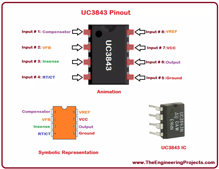
Hello everyone! I hope you all will be absolutely fine and having fun. I am going to give you the detailed discussion about Introduction to UC3843 today. UC 843 is basically a current mode Pulse Width Modulation (PWM) controller having fixed frequency. It is basically designed for DC to DC converter purposes as well as off line applications and it requires minimum external components. UC-3843 has three different packages which will be explained later. UC-3843 has several different features which make it ideal and useful for a lot of real life applications. These features may include trimmed oscillator for the control of accurate duty cycle, high gain amplifier and to control power MOSFET, there is a high current totem-pole output. Moreover, some other features include temperature compensated reference and current sensing. UC 3843 can be used at several different places e.g.in switching regulators having any of the polarities as well as in transformer coupled DC to DC converters. The further detail about UC-3843 will be given later in this tutorial.

Introduction to UC3843

UC3843 is basically a current mode Pulse Width Modulation controller. It is specially designed for DC to DC converters and off line application purposes. This device performs its tasks with minimal requirement of external components to avoid complexity. It is most common due to its unique features including current sensing, high gain amplifiers, high current totem-pole out for the control of MOSFET. UC-3843 can be used in transformer coupled DC to DC converters etc. UC-3843 is shown in the figure given below.
1. UC3843 Pins
  • UC-3843 has eight (8) input and output pins, four pins are on left side and the other four on the right side of the IC.
  • UC 3843 all pins are given in the table shown in the figure below.
2. UC3843 Pins Description
  • We can not use any device until we do not know about the functions of each and every pin.
  • So, I have provided the function associated with each of the individual pin, in the table shown below.
3. UC3843 Pinout
  • Pin configurations are very much necessary to understand in order to properly operate a device.
  • UC-3843 pinout diagram is presented in the figure given below.
4. UC3843 Packages
  • Packages are usually used to denote the different versions or models of the same device.
  • UC-3843 has three different packages, I have provided all of its packages in the table shown in the figure below.
5. UC3843 Packages Dimensions
  • The size of each model is kept different from each other in order to differentiate them easily.
  • All the packages of UC 3843 along with their dimensions are given in the table shown in the figure below.
6. UC3843 Amplification Circuit
  • We can perform amplification tasks by using the PWM controller named as UC 3843. The design of amplification circuit using UC-3843 is shown in the figure below.
7. UC3843 Ratings
  • To know about the amount of necessary parameters e.g power, voltage and current.
  • UC 3843 ratings are listed in the figure shown below.
8. UC3843 Features
  • Features are one of the most important features that can make a device popular, if they are unique.
  • UC 3843 main features are listed in the figure shown below.
9. UC3843 Applications
  • A device, most of the time is known on the basis of its applications and they play a vital role in its market.
  • UC-3843 some of the common applications are provided in the table shown in the figure below.
The Tutorial Introduction to UC3843 has basically focused on the basic use of the UC 3843 PWM controller. The parameters like pins, pins configurations, packages & their dimensions, ratings, features and application are focused. I hope that this tutorial will prove itself to be an informative article for you. If find something unclear or missing, please let me know, I will immediately update it so it could help more users. I will share further informative topics with you, in my upcoming tutorials. So, till then take care :)

Introduction to LM311

Hello everyone! I hope you all will be absolutely fine and having fun. Today, I will share the details discussion on Introduction to LM311. LM 311 is basically a voltage comparator having high speed. It can operate over wide ranges of voltage i.e. from -15V to15V, in case of operational amplifier. LM-311 can also operate on 5V for the logic systems. LM-311 output levels has the compatibility with Transistor Transistor Logic (TTL) levels circuits. At 50mA and at 50V too, LM-311 can operate lamps and relays. LM 311 can operate from 0 degree Celsius to 70 degree Celsius. LM-311 has several different features. These features include fast response time, strobe capability, wide voltage supply ranges, maximum input current, operating at single 5V power supply ranges, low power consumption, large input differential voltages etc. Several different applications are associated with LM 311 IC. These applications may include peak detectors, personal computers, white goods, building automation, body control modules etc. The further detail about LM-311 will be given later in this tutorial. [otw_is sidebar=otw-sidebar-7]

Introduction to LM311

LM311 is a voltage comparator with high speed. It is able to perform tasks over a large range of voltages. Its output levels are compatible with MOS circuits. Relays and lamps can be controlled by LM 311 when it is operating at 50V and 50mA as well. LM-311 has a lot of features like low power consumption, wide operating voltages, strobe capability, maximum input response time. It can be used in building automation, personal computers, white goods, embedded systems etc. LM-311 is shown in the figure below.
1. LM311 Pins
  • LM 311 has total eight pins, 4 on left side and 4 on the right side of the IC.
  • These pins are provided in the table shown in the figure below.
2. LM311 Pins Description
  • Each pins is assigned with the different task to be performed by the IC.
  • The tasks assigned to each of the pin are listed in the table shown in the figure below.
3. LM311 Pinout
  • Before using any device, we must know about its pin configurations.
  • We can understand pin configurations from the pinout diagram of that particular device.
  • LM-311 pinout diagram is shown in the figure given below.
4. LM311 Packages
  • The different models of a device are usually know as its packages, used to differentiate the latest products as compared to the earlier.
  • LM 311 has five different models which are given in the table shown in the figure given below.
5. LM311 Packages Dimensions
  • Every package is assigned with different dimensions in order to differentiate them easily.
  • LM-311 all packages are given in the table shown in the figure below.
6. LM311 Symbolic Representation
  • Symbolic representation of any electronic device shows the internal structure of that particular device.
  • LM 311 symbolic representation is shown in the figure below.
7. LM311 Schematic
  • Schematic diagram helps us to understand the internal functions of an equipment.
  • LM 311 schematic diagram is displayed in the figure shown below.
8. LM311 Ratings
  • Power requirements of a device are necessary to estimate for its proper operation.
  • LM-311 all types of ratings are listed in the table shown in the figure given below.
9. LM311 Features
  • A device can be considered a ideal on the basis of its amazing as well as unique feature from all other such devices.
  • LM 311 features are provided in the table given in the figure shown below.
10. LM311 Applications
  • On industrial scale any device is recognized from its applications, so applications play a vital role in the importance of any device.
  • LM-311 major and most common applications are provided in the table shown below.
In this tutorial Introduction to LM311, I have tried my best to cover all the necessary information about the basic use of LM 311, which include its pins along with configuration, its symbolic representation, ratings, features, applications and a lot more. I hope you have enjoyed this article and will appreciate my effort to do that. It will boost me up to do better better in future. Information about many other IC's will be provided in my later tutorials. So till then take care and bye :)

Introduction to LM224

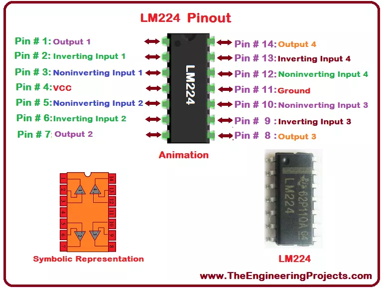
Hello everyone! I hope you all will be absolutely fine and having fun. Today, I will provide you document on detailed discussion about Introduction to LM224. LM-224 has four internal builtin operational amplifiers. These amplifiers are frequency compensated. The basic purpose to design these type of device is to operate it from a single power supply sources. Moreover, they are also able to perform different tasks using split power supplies. Magnitude of power supply and the current current drain both are independent of each other. LM-224 has a very wide range of application areas which include DC gain blocks, transducer amplifiers etc. LM 224 has a large number of amazing features include wide power supply ranges, large bandwidth, low input offset voltage, low input biasing current, common mode input voltage includes ground as well, high voltage output swing and many others. LM 224 also has a very wide range of real life applications. LCD and digital TV's, digital multi-meters, oscilloscope, weigh scales, DVD recorders, DVD players, chemical sensors, gas sensors, temperature sensors etc are the most common examples of the applications of LM-224 integrated circuit. The further detail about LM-224 will be provided later in this article.

Introduction to LM224

There are 4 internal operational amplifiers in LM224 IC. These amplifiers are internally frequency compensated. They are cable of operating using both single power supply sources as well as split power supply sources. It is the most common device due to its excellent features including low cost and high performance parameters. It features include large bandwidth, low input offset voltage and current, low input bias current etc. It can be used in LCD TV's, multi-meters, temperature sensors and a lot more. LM-224 is shown in the figure given below.
1. LM224 Pins
  • LM-224 has total fourteen (14) pins, each single pin has different functionality.
  • The names of all the pins are provided in the table shown in the figure given below.
2. LM224 Pins Description
  • LM-224 each single pin has different functionality.
  • The description of each pin is provided in the table shown in the figure given below.
3. LM224 Pinout
  • We can get information about pins configurations of any device using its pinout diagram.
  • LM-224 pinout diagram is shown in the figure given below.
4. LM224 Packages
  • If a device has its different models, they can be denoted by its packages.
  • LM-224 packages are given in the table shown below.
5. LM224 Packages Dimensions
  • Each package is provided with a different dimension.
  • LM-224 packages with different dimensions are given in the table below.
6. LM224 Symbolic Diagram
  • If we want to view the internal structure of any device, we must look at its symbolic representation.
  • LM 224 symbolic diagram is shown in the figure given below.
7. LM224 Ratings
  • The current, power & voltage requirement of a device can be estimated through its ratings.
  • LM-224 ratings are listed in the table shown in the figure given below.
8. LM224 Features
  • We can judge the performance of any device on the basis of its features.
  • LM 224 basic features are provided in the table shown in the figure below.
9. LM224 Applications
  • LM 224 has several different applications associated wit the real life.
  • Some of the applications are listed in the table shown in the figure below.
In the tutorial Introduction to LM224 I have provided the basic information about LM 224 IC. I hope you enjoyed the tutorial. If ypu find any problem you can ask us in comments anytime. I will share other topics in my upcoming tutorials. Till then take care :)

Introduction to LF351

Hello everyone! I hope you all will be absolutely fine and having fun. Today, I will give an elaboration about Introduction to LF351. LF-351 is basically JFET (Junction Field Effect Transistor). It is a very high speed input Op-amp (Operational Amplifier). This device is most common in the market due to its low cost and good performance characteristics. LF-351 provides a high gain bandwidth product even though it needs a very low current supply. LM 351 also provides higher slew rates. This device is most of the times known on the basis of its applications. LM-351 is the most popular device due to its unique features. These features include low input bias current, high gain bandwidth product, loww current supply, high input impedance, internal trimmed offset voltage, quick settling time, low harmonic distortion etc. Moreover, LM-351 can be use at different places e.g. circuits that need high input impedance, integrators with high speed, quick digital to analog converters, sample and hold circuits etc. The further detail about the operational amplifier LM-351 will be given later in this article.

Introduction to LF351

LF351 is basically JFET input operational amplifier. It is a low cost device and provides high performance characteristics. It can provide higher slew rates as well as high gain bandwidth product even by operating with a very low current supply. Moreover, it has internal compensated input off-set voltage. low current supply, high input impedance, quick settling time, low harmonic distortion are few of its main features. We can use this device while designing digital to analog converters, high speed integrators, sample & hold circuits etc. LM-351 is shown in the figure given below.
1. LF351 Pins
[ultimate_spacer height=”10”]
  • There are total eight (8) pins in an operational amplifier named as LF351.
  • LF 351 pins are given in the table shown in the figure given below.
2. LF351 Pin Description
[ultimate_spacer height=”10”]
  • We can't perform anything and even can't get the desired results if we don't know about the functions of pins .
  • LF-351 pins functions are shown in the table given in the figure given below.
3. LF351 Pinout
[ultimate_spacer height=”10”]
  • If we wanna know about the configurations of individual pin, we must have a look at the pinout diagram of an electronic device, usually provided along with that device.
  • LF -351 pinout diagram is given in the figure shown below.
4. LF351 Symbolic Representation
[ultimate_spacer height=”10”]
  • In order to view the internal structure of a device we should have a look at its symbolic diagram.
  • LF 351 symbolic form is given in the figure shown below.
 
5. LF351 Schematic Diagram
[ultimate_spacer height=”10”]
  • Schematic diagram provides us help in understanding the internal circuitry of any of the electronic device.
  • LF 351 schematic diagram is given in the figure shown below.
6. LF411 Ratings
[ultimate_spacer height=”10”]
  • The ratings are very helpful while estimating the power requirement of an electronic device.
  • LF 351 all ratings are shown in the table given in the figure given below.
7. LF411 Features
[ultimate_spacer height=”10”]
  • Features play a vital role in the popularity of a device.
  • LF 351 some of the major features are shown in the table given in the figure below.
8. LF411 Applications
[ultimate_spacer height=”10”]
  • LF-351 has several different of real life applications, some of them are shown in the table given below.
The tutorial Introduction to LF351 provides you the detailed discussion on the very basic and starting use of an operational amplifier named as LF-351. The discussion includes the applications, features, symbolic representation and a lot more about this device. I hope you will enjoy this tutorial and will appreciate my effort. I would like to share many of the other informative topic with you guys in my upcoming tutorials. So till then take care & bye :)

Introduction to LM4040

Hello everyone! I hope you all will be absolutely fine and having fun. Today, I am going to give a detailed discussion on Introduction to LM4040. LM-4040 is specially designed for an accurate micro-power shunt voltage reference. These voltage references includes the standards of 2.5V, 3V % 5V respectively. LM-4040 has three different grade A, B and grades and they have o.1%, o.5% and 1% tolerances respectively. This device is available in different packages and each package has different individual dimension which will be explained later. We can achieve an excellent performance from this device when it is operating at the current ranging from 60uA to 15mA and its temperature coefficient is 20 ppm per degree. In order to maintain good stability level the device's design is much tolerant to capacitive loads. LM-4040 has several different features e.g. low output noise, no output capacitor, good output voltage tolerance, large current operating ranges, low temperature coefficient, lead (Pb) free, halogen free, antimony free etc. It can be used at different places like battery powered systems, portable communication devices, notebook and palm-top computers, portable instrumentation, accurate power supply, data acquisition systems etc. The further detail about LM 4040 will be given later in this tutorial.

Introduction to LM4040

LM4040 is a device which is designed to achieve accurate micro-power shunt voltage references e.g. 2.5V, 3V and 5V. It has three different grades, each having different individual tolerances. The device is available in different packages. LM-4040 has different features e.g. low output noise, large operating current ranges, good output voltage tolerance etc. Moreover, it can be used in battery powered systems, computers, portable instrumentation and at lot more places. LM-4040 is shown in the figure given below.
1. LM4040 Pins
  • This device has three pins in total, 2 input and a single output pin.
  • LM-4040 pins are listed in the table shown in figure below.
2. LM4040 Pins Description
  • Each of the single pin has its different individual function which is necessary to be known.
  • LM-4040 pins description are given in the table shown in the figure below.
3. LM4040 Pinout
  • Pinout diagram presents the pins configurations of an electronic device.
  • LM-4040 pinout diagram is shown in the figure given below.
4. LM4040 Packages
  • Different versions of a same device can be denoted by its packages.
  • LM-4040 packages are provided in the table shown in the figure below.
5. LM4040 Packages Dimensions
  • Each package has different individual dimensions in order to differentiate easily.
  • LM-4040 package dimensions are listed in the table shown in the figure given below.
6. LM4040 Symbolic Representation
  • If we want to know about internal structure of any device, we must see its symbolic representation.
  • LM-4040 symbolic representation is shown in the figure given below.
7. LM4040 Ratings
  • Power requirement of a device can be seen through its rating.
  • LM-4040 ratings are listed in the table shown in the figure given below.
8. LM4040 Features
  • Features are very important parameters which can make a device more and more popular.
  • LM-4040 features are listed in the table given in the figure shown below,
9. LM4040 Applications
  • Applications are the most important parameter of a device that can make it ideal for some or for a lot of purposes.
  • LM-4040 applications are given in the table shown in the figure below.
  • The shunt reference circuit can also be designed using LM 4040 and it is its most typical application as well.
  • LM-4040 typical shunt reference designed circuit is shown in the figure given below.
  • You can see that only a shunt resistance is added to LM 4040 for its shunt reference.
That's all the discussion about Introduction to LM4040. The major part of the discussion consist of the main point like LM 4040 pins, configurations, its features, applications and a lot more was also discussed in this tutorial. I hope this tutorial has proved to be an informative and exciting tutorial for you guys. If you have any sort of problem you can ask us in comments any time. Our team is always there to help you. If you found something missing in this article, please let me know, so that I can update this article immediately. I will share my tutorials on several different informative topics later. Till then take care :)

Introduction to LM293

Hello everyone! I hope you all will be absolutely fine and having fun. Today, I am going to give you an elaboration on Introduction to LM293 an Integrated Circuit (IC). LM-293 is a dual independent accurate voltage comparator. LM 293 has a capability to perform its operation from a single supply source as well as from split power supply. The purpose to design LM-293 is to permit a common mode range to the ground level and it perform this operation with single power supply source. LM-293 is the most common device in the market these days due to its high performance and cost effectiveness. This device is considered to be an ideal for a lot of electronics applications. LM-293 has a lot of features which make it different from all other devices. These features include low input offset voltage, low input offset current, low input bias current, wide voltage supply ranges, power supply equal to differential input voltage ranges, lead (Pb) free and lot more. LM-293 can be used at several different places in real life. It can be used in gas sensors, chemical sensors, weigh scales, AC induction, personal computers etc. The further details about LM-293 will be given later in this tutorial.

Introduction to LM293

LM293 is basically a dual independent voltage comparator. It can perform its operations through a single power supply source as well as through split power supplies. It is a low cost device and is easily available in the market now a days. It has a lot of features including wide voltage supply ranges, low input offset current, low input bias current etc.Moreover, it can be used in chemical sensors, personal computers etc. LM-293 is shown in the figure given below.
1. LM293 Pins
  • LM-293 has total eight (8) pins, each has its own feature different from the other.
  • All of the pins of LM 293 are listed in the table shown in the figure below.
2. LM293 Pins Description
  • Each pin has its different functions and we must know about each of the function.
  • LM-293 pins functions are given in the table shown in the figure below.
3. LM293 Pinout
  • Pinout diagram of an electronic device helps to understand its pins configurations for its appropriate use.
  • LM-293 pinout diagram is shown in the figure given below.
4. LM293 Packages
  • Packages are developed to show the different models of the same device.
  • LM-293 packages are given in the table shown in the figure below.
5. LM293 Packages Dimensions
  • Different dimensions are usually assigned to different packages in order to differentiate them easily.
  • LM-293 packages dimensions are listed in the table shown in the figure given below.
6. LM293 Schematic Diagram
  • LM-293 schematic diagram is shown in the figure given below.
  • It helps us to understand the internal circuit diagram of any of the electronic device.
7. LM293 Symbolic Diagram
  • Symbol diagram shows the internal structure of any device.
  • LM-293 symbolic representation is given in the figure shown below.
8. LM293 Ratings
  • Ratings display the amount of voltage, current and power required by an electronic device.
  • LM-293 ratings are listed in the table shown in the figure given below.
9. LM293 Features
  • Features are such parameters which can make a device popular in the market.
  • LM-293 major features are listed in the table shown in the figure given below.
10. LM293 Applications
  • LM-293 has several different real life applications.
  • A few of the major applications are shown in the table given in the figure below.
The tutorial Introduction to LM293 has provided the detailed discussion about the basics methods of using a specific Integrated Circuit (IC) named as LM-293 IC. I have tried to provide all the necessary information about the particular IC, if you founf something missing, please let me know so that I can immediately update it. If you feel any sort of problem you can ask me anytime in comments. Our team and me are always there to help you. I will share further informative topics with you guys in my upcoming tutorials. Till then take care & bye :)

Introduction to LM380

Hello everyone! I hope you all will be absolutely fine and having fun. Today, I am going to share my knowledge about Introduction to LM380. LM-380 is an audio amplifier, specially designed for the customer's power audio amplification purposes. Its designers fix its gain internally up to 34dB. In LM 380, ground reference signal is allowed by a unique input stage and the output automatically maintains its level to half of the supplied input voltage. LM-380 has a copper lead frame. The three pins in the middle of the IC on both side, are basically the ground pins. These three pins on both sides makes it easy for the user to use this device for standard PC's. LM 380 has several different features e.g. wide supply voltage range, high peak current, low distortion etc. Moreover, LM 380 provides high input impedance, low quiescent power drain, fixed voltage gain, input referenced to ground etc and a lot more. LM-380 is the most common device and easily available in market now a days due to its cost effectiveness and high performance. LM 380 can be used at different places in real life. Its applications may include intercoms, ultrasonic drivers, line drivers, teaching machine output, television sound systems, alarms, phonograph amplifiers etc. Some other applications include power converters, AM radio, FM radio, servo motor drivers etc. The further detail about LM-380 will be given later in this tutorial. [otw_is sidebar=otw-sidebar-7]

Introduction to LM380

LM380 is an audio amplifier used specially for power audio amplification purposes. It has a fixed internal gain. A specific input signal allows ground reference signal and the out signal maintains its level to the half of the applied input voltage. Three ground pins on both sides of the IC make its use easier for anyone to use it. wide supply voltage ranges, high peak current, high input impedance, low distortion are its major features. LM-380 can be used in intercoms, servo motors drivers, alarms, TV sound systems etc. LM 380 IC is shown in the figure given below.
1. LM380 Pins
  • Pins of a device play a vital role for applying any sort of input and to achieve the desired output.
  • LM-380 has fourteen (14) pins, each individual pin has its own importance.
  • All these pins are provided in the table shown in the figure below.
2. LM380 Pins Description
  • In LM 380 six pins are such that they have their common functions, and they are the ground pins.
  • Pins play a very important role when we desire to achieve the particular results from that device.
  • LM-380 pins description is given in the table shown below.
3. LM380 Pinout
  • Pinout diagram helps us to understand the pin configurations of a device.
  • We must have a look at pinout diagram of any device before going to use it.
  • LM-380 pinout diagram is shown in the figure given below.
4. LM380 Symbolic Representation
  • Through symbolic form of a device, we can understand the internal structure of that particular device.
  • LM-380 symbolic representation is shown in the figure given below.
5. LM380 Schematic Diagram
  • Through schematic diagram we can understand the internal flow of the capability of a device to perform different tasks.
  • :LM-380 schematic representation is given in the figure shown below.
6. LM380 Ratings
  • We always need a power supply to operate any device, and the characteristics of that supply totally depends upon the ratings of the device.
  • LM-380 ratings are listed in the table shown in the figure below.
7. LM380 Features
  • Features are such a property of any device that can make it more and more popular if they are unique.
  • LM-380 some of the common features are given in the table shown in the figure below.
9. LM380 Applications
  • Now a days most of devices are commonly know on the basis of their applications i.e they play also an important role.
  • LM-380 some of the major uses are listed in the table shown below.
The tutorial Introduction to LM380 has elaborated the thing necessary for the basic use of integrated circuits such as LM-380. The main focus of this article is to facilitate the user by providing a better understanding for the use if the particular device. I have tried to cover all the important details, if I have missed something, please let me know the. So, that I can update this article as soon as possible for the future ease. I hope you have enjoyed this tutorial. I will surely share further informative topics with you guys in my later upcoming tutorials. Till the take care and bye :)

Introduction to LF411

Hello everyone! I hope you all will be absolutely fine and having fun. Today, I am going to give a detailed discussion on Introduction to LF411. LF-411 is a Junction Field Effect Transistor (JFET) input Operational Amplifier (Op-amp). It is the most common module available in the market these days due to its cost efficiency. LF 411 has low input offset voltage. Input offset voltage drift is guaranteed for LF-411. A very low supply current is needed for this device. It provides higher slew rates as well as high gain bandwidth product. Moreover, LF411 also provides lower input bias current as well as lower input offset currents. It is an 8 pin operational amplifier. The details about its pins will be discussed later. Due to its low cost and high performance efficiency it is most common device and is easily available in the market these days. LF-411 has several features which make it the most common device in today’s market. These features include high slew rates, fast settling time, high input impedance, input offset voltage drift etc. Moreover, its other major features consists of internal trimmed offset voltage, low supply current, low input bias current, low input offset current, wide gain bandwidth product, low harmonic distortion etc. LF-411 can be used in high speed integrators, sample and hold circuits, high speed digital to analog converters etc. The further detail about LF-411 will be given later in this tutorial.

Introduction to LF411

LF411 is basically a Junction Field Effect Transistor (JFET) input operational amplifier. It is a low cost device and easily available in the market. It is usually know on the basis of its applications. It requires very low current supply and provides higher slew rates and high gain bandwidth product in response. It also provides input offset voltage drift. Low harmonic distortion, high input impedance, high slew rates are some of its features. It can be used in high speed integrators, sample and hold circuits etc. LF-411 is given in the figure shown below.
1. LF411 Pins
[ultimate_spacer height=”10”]
  • There are total 8 pins in the operational amplifier LF411.
  • LF-411 pins are listed in the table shown in the figure given below.
2. LF411 Pins Description
[ultimate_spacer height=”10”]
  • We can not perform any task and can not get appropriate results if we do not know about the pin’s function.
  • LF 411 pin functions are listed in the table shown in the figure given below.
3. LF411 Pinout
[ultimate_spacer height=”10”]
  • If we want to know about the configuration of the individual pin, we must see the pinout diagram of any electronic device, provided along with that device.
  • LF 411 pinout diagram is shown in the figure given below.
4. LF411 Package
[ultimate_spacer height=”10”]
  • A device’s different models/versions can be presented through its packages.
  • LF-411 has only a single 8 pins package, as given in the table shown in the figure below.
5. LF411 Package Dimension
[ultimate_spacer height=”10”]
  • LF 411 package dimension along with the SI units is given in the table shown in the figure below.
6. LF411 Symbolic Representation
[ultimate_spacer height=”10”]
  • To view the internal structure of a device we must have a look at its symbolic form.
  • LF-411 symbolic form is shown in the figure given below.
7. LF411 Schematic Diagram
[ultimate_spacer height=”10”]
  • Schematic diagram helps us to understand the internal circuitry of an electronic device.
  • LF-411 schematic diagram is shown in the figure below.
8. LF411 Ratings
[ultimate_spacer height=”10”]
  • Ratings are helpful in estimating the power requirement of any device.
  • LF-411 ratings are listed in the table shown in the figure given below.
9. LF411 Features
[ultimate_spacer height=”10”]
  • LF-411 some of the standard features are provided in the table shown in the figure below.
10. LF411 Applications
[ultimate_spacer height=”10”]
  • LF 411 has a lot of real life applications, some of them are listed in the table shown below.
The article Introduction to LF411 has provided you the detailed discussion on the basic use of an operational amplifier named as LF 411. The aim was to facilitate the engineering students who want to use this device in their projects. If you found something missing, please let us know as soon as possible so that the tutorial could be updated correspondingly. I will also share other informative topics with you, for sure. So, till then, take care :)
Syed Zain Nasir

I am Syed Zain Nasir, the founder of <a href=https://www.TheEngineeringProjects.com/>The Engineering Projects</a> (TEP). I am a programmer since 2009 before that I just search things, make small projects and now I am sharing my knowledge through this platform.I also work as a freelancer and did many projects related to programming and electrical circuitry. <a href=https://plus.google.com/+SyedZainNasir/>My Google Profile+</a>

Share
Published by
Syed Zain Nasir