Introduction to PCB(Printed Circuit Board)
Hello everyone, I hope you all are doing great. Today, I am going to start a new tutorial series on Printed Circuit Boards, abbreviated as PCB. It's going to be a quite lengthy series so I have divided it into multiple chapters. We will start from the basics and will gradually move towards complex concepts. In this series, we will cover everything related to PCB i.e. PCB Types, materials used in PCB designing, online software and tools to design PCB layouts, online PCB Fabrication Houses to manufacture PCB etc. So, stay tuned to this series, if you want to be a PCB expert.
As today's our first chapter in this series, so we will discuss the basics of PCB i.e. What is PCB? History of PCB? How its evolved from simple boards to complex designs? What makes it useful in the latest technology? etc. So, let's hop on the board and dive in the details of PCB:
Introduction to PCB
- PCB is an acronym for Printed Circuit Board used to connect the electronics components with each other using pads and tracks incorporated on a laminated copper sheet.
- In simple words, a copper layer is laminated on an insulating sheet/board(developed using epoxy) and we place electronic components on this board.
- The copper layer has:
- Tracks: to allow the current flow from one component to another.
- Pads: to connect/solder electronic components to these tracks.
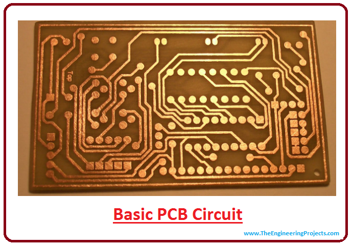
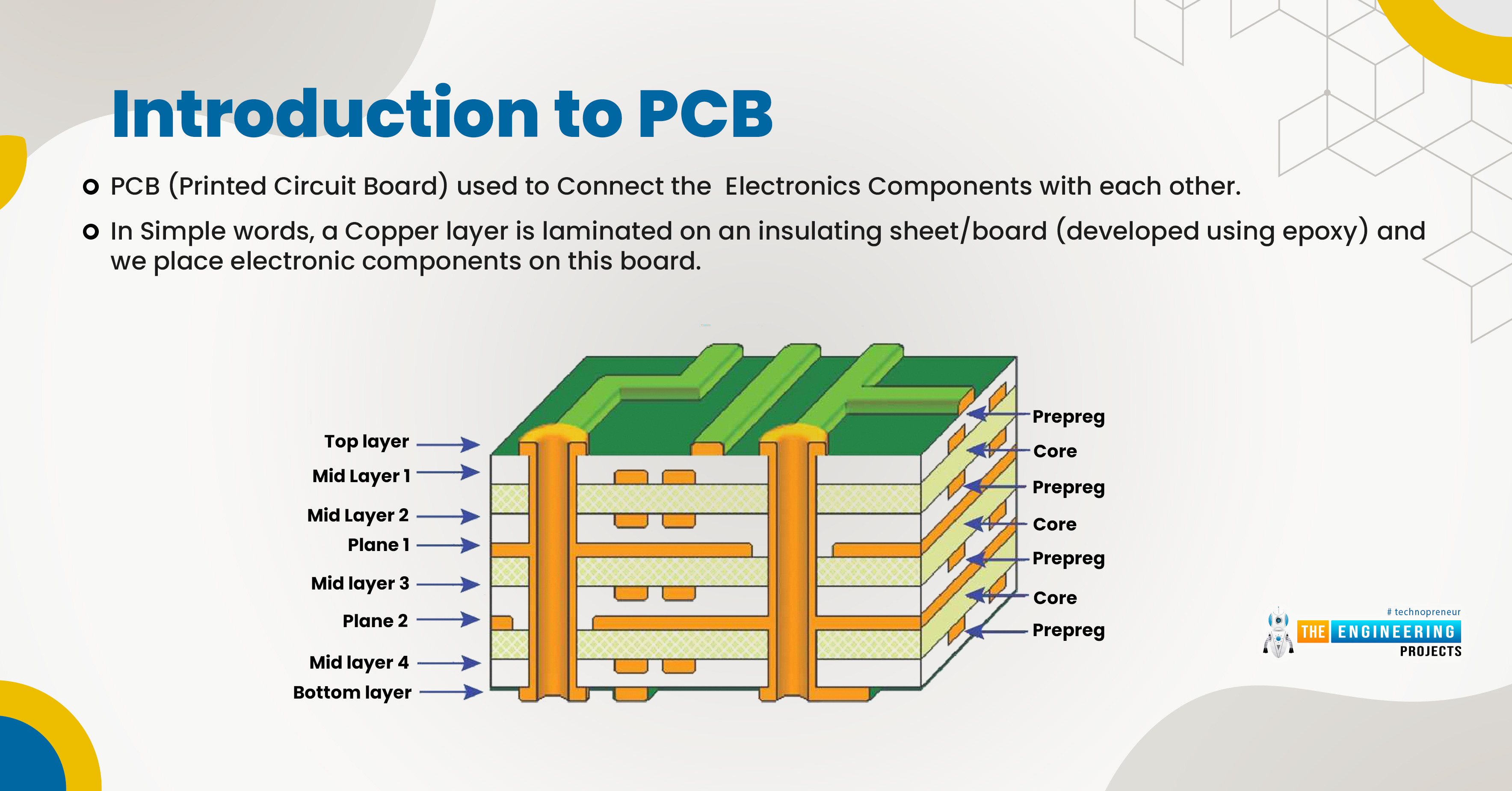
- A simple PCB board with labels is shown in the below figure.
Why do we need PCB?
- If you have worked on any electronics projects, you must have the idea of Breadboard and Verboard. Both of them are used to create electronic circuits.
- Breadboard is used normally for academic purposes i.e. when you want to study the behavior of electronic circuits. We just place our components on the breadboard and get the desired output.
- In the case of Veroboard, we need to solder these components, in order to make our circuit work and it's normally used in custom-build projects, where you need to design the circuit once.
- But what if, you are designing a product and you want these circuits in bulk? That's where PCB comes into action.
How to design a PCB?
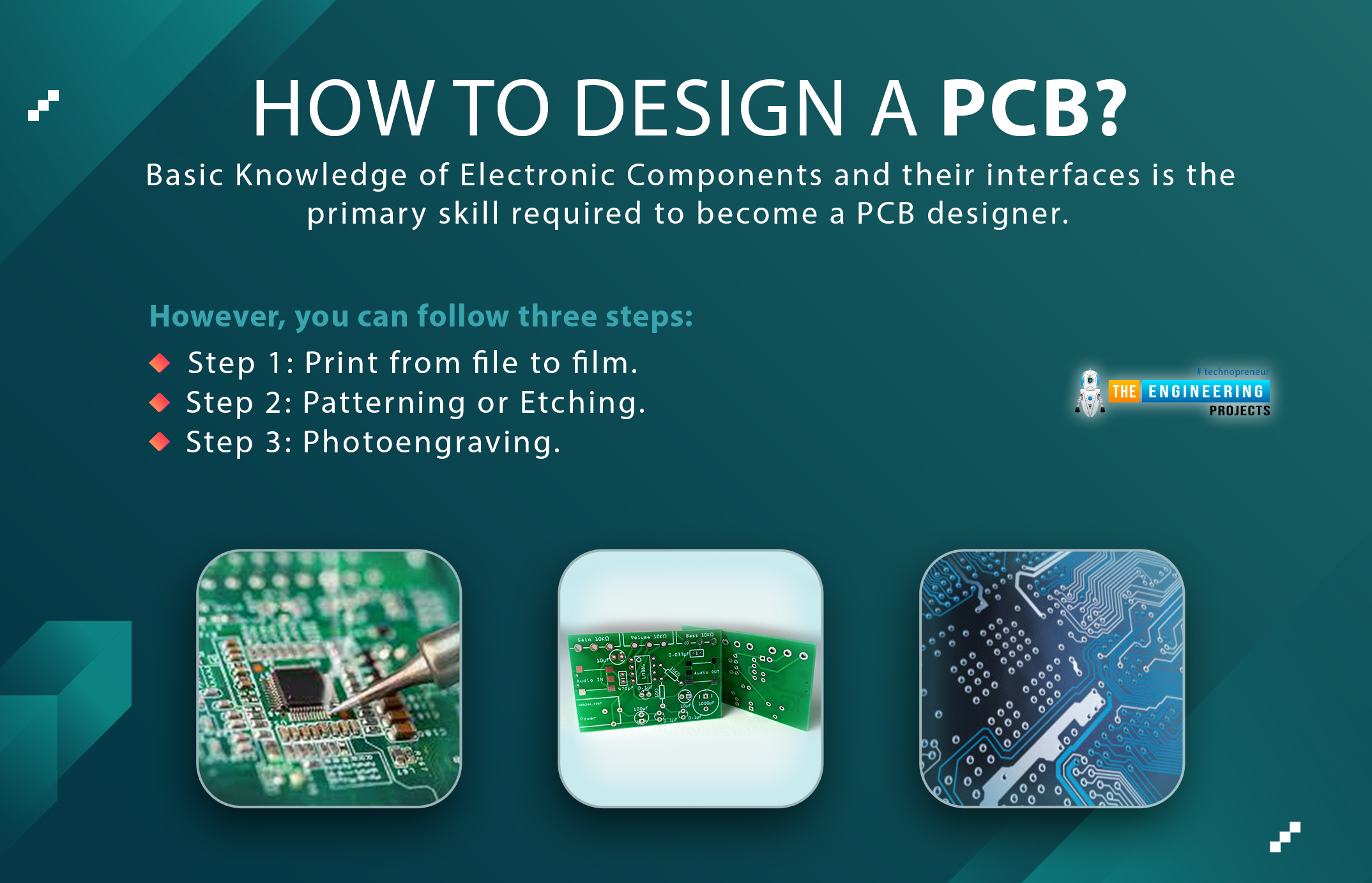
- In order to design a PCB, you should have a complete understanding of electronics.
- Suppose, I want to design a PCB of a DC Motor driver, first of all, I should have a complete understanding of its circuit and that's where we use Breadboard/Veroboard.
- So, before designing a PCB, you should first create a prototype to test the working of your circuit.
- Once you are satisfied with your circuit's working/output, then move towards designing its PCB.
- In the PCB designing process, the first thing we need to do is to create a software image of the PCB circuit.
- There are different software available for PCB designing i.e. Altium, KiCAD, FreeCAD etc. (We will cover these software in our upcoming chapters)
- Once your PCB design is ready, you will get its design files and will place an order at any PCB Fabrication House.
- We can also develop a PCB board from its design on our own(will cover that) but it's always recommended to place the order on some online PCB company.
- You will get local PCB manufacturing companies as well but I would suggest you to try online PCB companies i.e. JLCPCB, PCBWay, AllPCB, PCBOnline etc.
History of PCB
Before the inception of PCB, professionals used laborious methods of point-to-point wiring, in order to connect the electronic components. This method was costly and led to complicated designs.
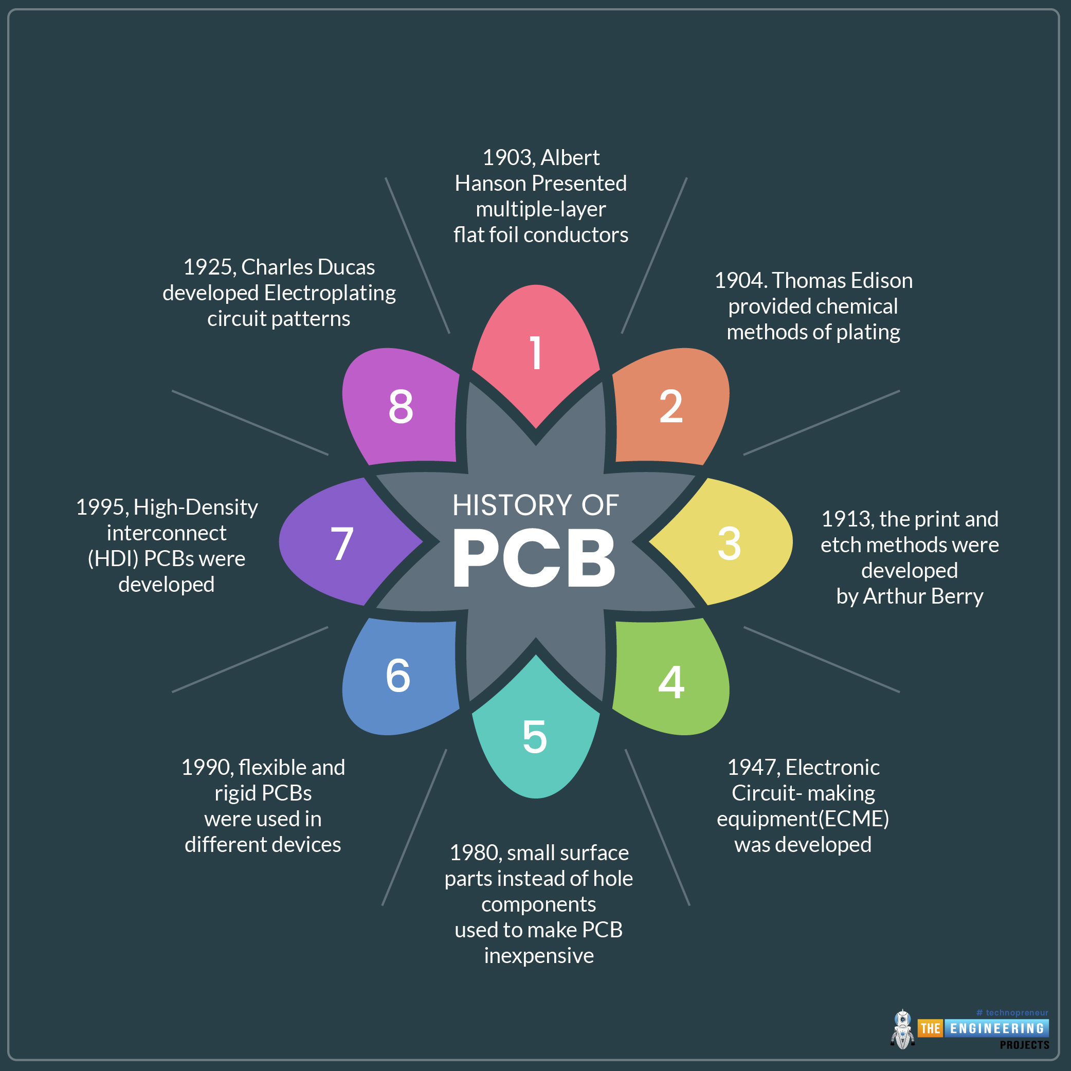
- In 1903, Albert Hanson presented multiple-layer flat foil conductors laminated on an insulator board.
- In 1904, Thomas Edison provided chemical methods of plating conductors on linen paper.
- In 1913, the print and etch methods were developed by Arthur Berry.
- In 1925, Charles Ducas developed electroplating circuit patterns.
- In 1936, Paul Eisler(an Australian Engineer) developed a printed circuit board as a part of the radio set.
- In 1941, a multi-layer printed circuit was developed.
- In 1943, during WW II PCB technology was used at a large scale to make proximity fuses.
- In 1947, electronic circuit-making equipment(ECME) was developed to produce three radio boards per minute.
- In 1949, the auto-assembly process is developed by Danko having component leads inserted into the interconnection pattern of copper foil and dip soldered.
- In 1952, Motorola adopted plated circuit board technology on a commercial level in home radios and announced an investment of $ 1M.
- In 1960, printed circuit boards with reduced weight, size and cost were introduced and used in radios.
- In 1980, small surface-mount parts were used instead of hole components to make PCB inexpensive.
- In 1984, the Institute of Electrical and electronics engineers( IEEE) awarded Harry W. Rubinstein an award for the development of printed components and conductors on a single insulating substrate.
- In 1990, flexible and rigid PCBs were used in different devices.
- In 1995, High-Density Interconnect(HDI) PCBs were developed.
- With the passage of time demands for electronics became prevalent, and this made professionals think they should come up with an ideal solution to make the electronics cheap and incorporated in a lesser space.
Composition of PCB
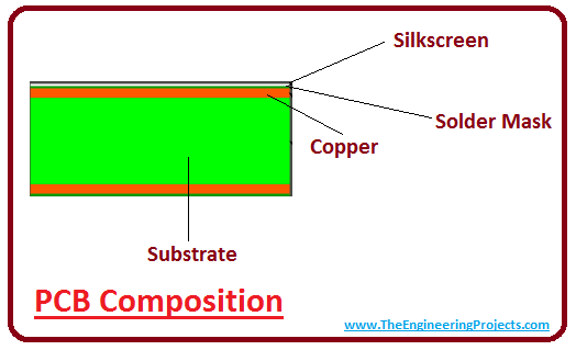
Now let's have a look at the composition of the PCB board. A simple PCB board is composed of different layers that are joined together with the help of heat and adhesive, giving the board a compact shape into a single object. These PCB board layers are named:
- Substrate Layer.
- Copper Layer.
- Solder Mask Layer.
- SilkScreen Layer.
Let's discuss each layer one by one.
Substrate Layer
- The base material, also known as substrate, is composed of fiber glass.
- The FR4 is the most common fiber glass used today. It is like a solid core that provides rigidity and thickness to the PCB board.
- Some PCB boards are composed of phenolics and epoxies which are not as durable as FR4 but they are less expensive and come with a unique bad smell.
- Low-end consumer electronics mostly use these types of substrates.
- Phenolics come with low decomposition temperature which allows these substrates to erupt and delaminate if solder is placed on board for a long duration of time.
- The nature of the substrate material defines whether the board will be a Flexible PCB or a Rigid PCB.
Copper Layer
- Besides the substrate, there exists a thin layer of copper foil.
- Heat and adhesive are used to laminate the copper foil on the board.
- Commonly, both sides of the substrate are laminated with copper especially in double-sided PCB, except in cheap electronics where only one side of the board is laminated with copper.
- The copper thickness varies from board to board and can be defined in ounces per square foot.
- The one ounce per square foot is suitable for most of the PCB, but applications, where we require more power, come with 2 or 3 ounces per square foot.
- Each inch per square encompasses 35 micrometers of thickness.
Solder Mask Layer
- Above the copper layer foil, there lies a solder mask layer.
- This layer is applied on the copper layer to insulate the copper layer from surroundings, in order to avoid conduction, if direct contact happens with some metal or conductive material.
- The most commonly used solder mask comes in green color, however, it's available in other colors as well.
Silkscreen Layer
- Above the solder mask layer, there exists a silkscreen layer that allows the user to add symbols and number for better understanding of the board.
- Silkscreen labels provide the clear indication of function of each pin and component soldered in the board.
- Silkscreen mostly comes in white color but there are also other colors available including red, grey, black, yellow etc.
- Common practice is using silkscreen in single color, as combination of different colors of silkscreen makes it difficult for the user to read the board properly.
PCB Characteristics
Though we have a lot to cover in this topic, which we will in our upcoming lectures but here I just want to mention two basic characteristics of PCB, as they are directly connected to its composition.
Through Hole Technology
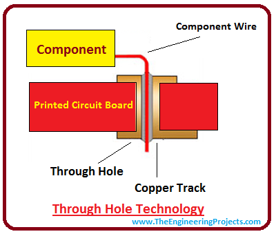
- In Through-hole technology, electronic components are mounted on the PCB board with leads inserted through holes. These leads are then soldered on the other side of the board and the ends are trimmed off.
- Through-hole technology is used in simple PCBs normally single-sided PCB and double-sided PCB.
-
Earlier PCBs were designed using through-hole technology.
Surface Mount Technology
- Surface mount technology came into play in the 1960s and became extensively popular till 1990.
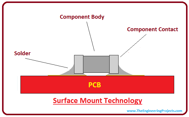
- In surface mount technology, SMD electronic components are used, which are quite small in size and instead of leads, these components have small pads, which are soldered into the PCB surface.
- Surface mount components are 10 times smaller than through-hole components, making them an ideal choice for complex and advanced applications.
- Components placement on both sides of the PCB is a common practice in Surface mount technology, providing a much larger circuit density with a relatively smaller PCB assembly.
- Surface mount devices have a leg over through-hole devices because of their low cost and simple design.
Types of PCB Boards
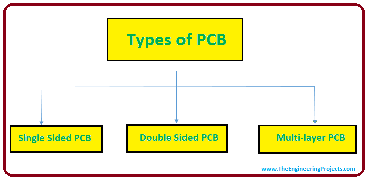
PCBs can be divided into different types depending on the nature and number of layers used in the boards. Let's have a quick look at a few of them. We will cover this in detail in our upcoming lectures.
Single-Sided PCB Boards
- Single-sided PCB boards came into play in 1950 and became an ideal choice for simple electronic circuits since then.
- In single-sided PCB boards, copper tracks are found on one side of the PCB board.
- Pins of electronic components are inserted from one side of the board to the other side that comes with copper tracks and lines.
- These pins are then soldered on the copper side in order to provide the conducting path to the components.
- These types of PCBs are commonly used in many electronic devices including printers, coffee machines, basic electronics circuits and calculators.
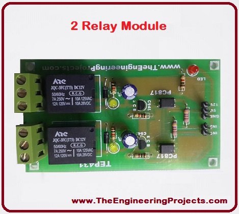
- I have posted a tutorial Interfacing of Arduino with 2 Relay Board, in that tutorial 2 Relay Board's PCB is Single Sided PCB and is shown below:
Double-Sided PCB Boards
- Double-sided PCB boards are served as a basic component for advanced technology applications.
- In these boards, copper tracks are applied on both sides of the boards.
- In order to provide a link between two points on both sides of the boards, holes are created on the boards and then laminated with the copper layer.
- The components on these boards are electrically connected using two techniques i.e. through hole or surface mount technology.
- Using through-hole technology, leads also known as wires are inserted in the hole and then each lead is connected to the right component and builds a smooth conducting path throughout the board surface.
- Wires don't behave as connectors in surface mount technology, instead, the whole board provides a wiring surface where small leads are directly connected to the board.
- Different functions can be accomplished at a much faster rate with less space using surface mount technology which helps in minimizing the cost and makes the whole project light-weight.
- Double-sided PCB boards are widely used in applications including amplifiers, vending machines, LED lighting, HVAC systems and general power supplies.
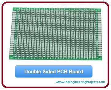
- Here's an image of Double Sided PCB Board:
Multi-layer PCB Boards
- Multilayer PCB boards are composed of a number of double-sided PCBs.
- These boards are then glued together with pieces of insulation in order to avoid excessive heat that can damage the components.
- Multi-layer PCBs come in different forms ranging from four layers to 16 layers or more.
- The thickest multi-layer PCB ever developed by professionals was 50 layers thick.
- These boards are more complex than double-layered PCBs, help in initializing faster operations than standard PCB boards and are very similar to microchip composition.
- Multi-layer boards are used in a wide range of applications including satellite systems, weather equipment, x-ray equipment, data storage, GPS technology and many more.
- I have discussed types of PCBs based on a number of layers, however, there are other types too like Aluminum PCB and High-Frequency PCB, but they are used for more robust applications where heat dissipation is required.
Applications of PCB
Now let's have a look at the real-life applications of printed circuit boards, to get an idea of their importance. We are literally surrounded by PCB boards, from mobile chargers to mobiles itself, from dentist machines to engineering cranes, every electronic machinery has a PCB board inside it. Let's discuss a few of them:
- PCBs are widely used in industrial machinery, where thick copper PCBs are installed in motor controllers, industrial load testers, high-current battery chargers, automated machinery etc.
- Advanced medical equipment uses high-density PCBs that provide a compact and smallest design possible. The small size and light weight of PCB beautifully replace the old traditional equipment and become an ideal choice for the medical field. These devices are useful for a range of applications from small components like pacemakers to large complex machines like X-Ray machines and CAT scanners.
- Aluminum-backed PCBs are widely used in LED-based lighting systems which encompass low power consumption and high level of efficiency. These PCBs are capable of transferring heat from one point to another and are considered a step ahead of standard PCBs. These PCBs are the backbone of basic lighting solutions and LED applications.
- Automotive and aerospace industries are widely surrounded by vibration environment, this is where flexible PCBs come into play. These PCBs can withstand high vibrations and severe environments due to their flexible and compact design. They can house in tight spaces like instrument gauges and instrument panels. Being lightweight makes it an ideal choice for manufacturing parts of transportation industries.


