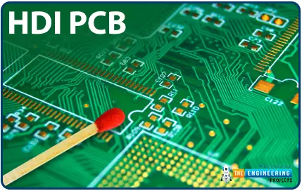
High Density Interconnect PCB


The printed circuit board is a type of plastic where electrical and electronic components lie, laminated and fixed. In modern days, there has been increasing in the complexity of electronic components and devices and this has also led to high demand for more complex PCBs that can make this achievable. This exclusive board that has been introduced in the market includes HDI, rigid-flex, Aluminium clad, buried and blind or even a blend of all the listed types.
There is a list of so many PCB types that a designer can choose for any type of electronic project ranging from single layer PCB to other complex types like the multilayered PCBs. In general, the simplest type of PCB contains copper tracks and interconnection between the elements and components on one side of the board. These types of boards are classified as single-sided boards or one-layer side of boards. However, there are other types of boards that are complicated and will require complex methods to do their designs. These boards are probably double-layered or even multilayered.
Multilayered boards are such complex boards that will require advanced technology for their manufacturing. This is where HDI boards come into play. HDI stands for High-Density Interconnect Boards. When addressing high density interconnect boards, we are focused on higher wiring density, the smaller vias, the thinner spaces and the higher pad density that accompany this type of board. This type of board has a lot of advantages over the typical circuit boards.
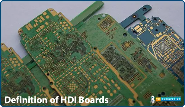
Definition of HDI Boards
PCBs are made up of components that are interconnected and fixed on them. The components are connected by wiring them on the board. The wiring is in form of tracks and traces. Some boards involve small low density of wiring capacity per unit area while others involve very high density wiring capacity per unit area. HID which is an abbreviation of the high density connect boards are boards that have a high density of the wiring capacity per the unit area when you compare with the normal PCBs.- These boards are very special as they come with finer lines, tiny vias and a high connection density of the pads than the one that is utilized in the normal boards.
- A good HDI PCB should have one or all of the following;
- Blind and buried vias
- Micro vias
- Build-up lamination
- Considerations of high signal performance.
- The HDI boards are very compact with small vias, micro-vias, spaces, pads and copper traces.
How to manufacture HDI PCB?
There are many online PCB companies that offer to manufacture High-Density PCBs. The one we highly recommend is PCBWay, china based PCB Manufacturing House. They offer the best quality product, within a specified time and have an excellent support team, ready to guide you throughout the process.- In order to manufacture HDI PCB, log in to the PCBWay official site.
- Now click on the PCB Calculator, and at the top click on Advanced PCB, as shown in the below figure:
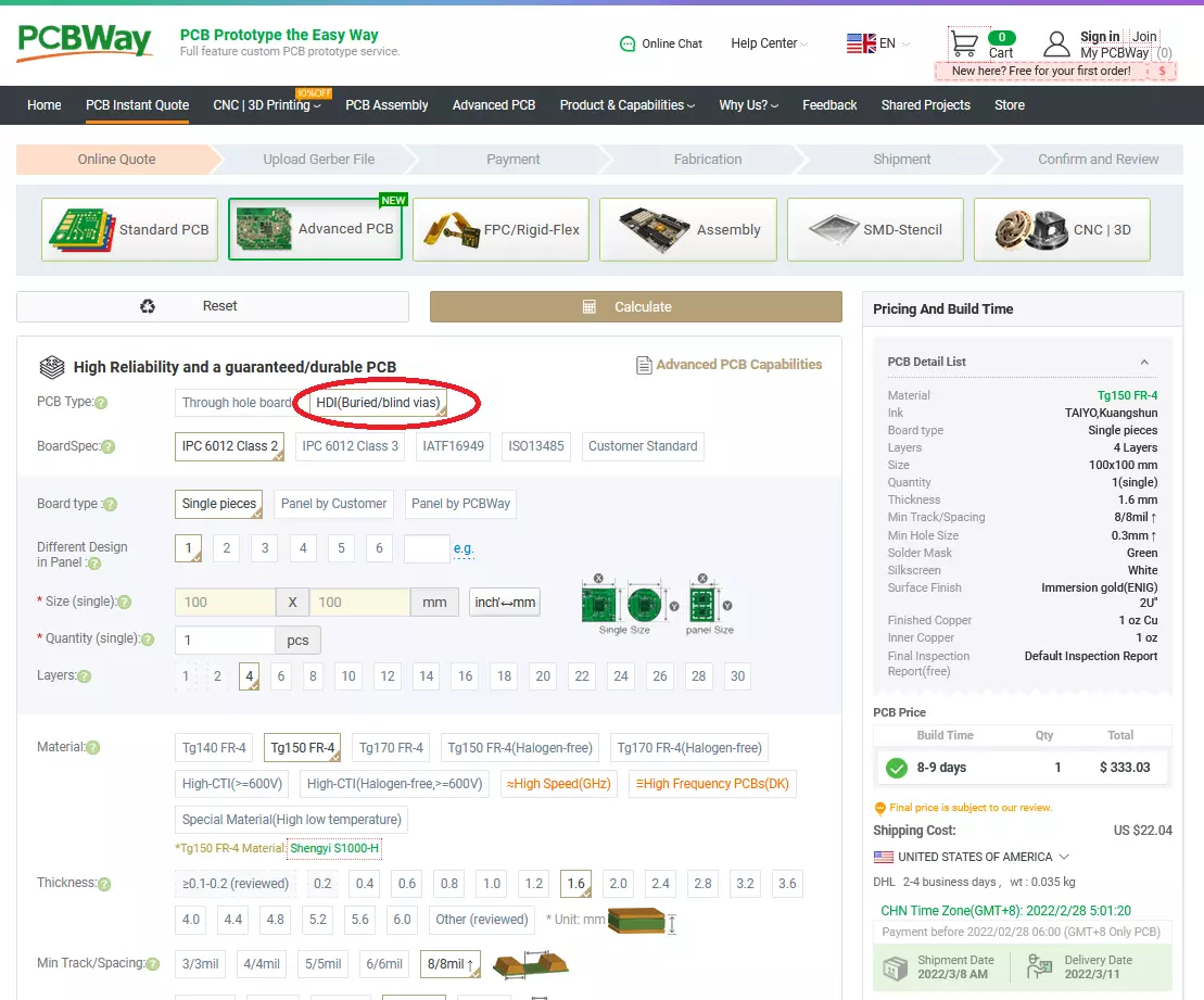
- In the PCB Type, select the HDI option, I have encircled it in the above figure.
- AS you can see for a single piece HDI PCB of size 100x100mm, the price is $333 and the shipping cost is $22 to USA.
- HDI PCBs are highly cost PCBs and are thus used in industrial products.
Variations in HDI PCBs.
HDI PCBs use vias and laser-drilled microvias to connect components between different multilayers. The microvias are the most preferred to offer the connections because they are much smaller and very effective when it comes to space utilization.
- We have at least five variations of the vias and microvias that can be used in the process of manufacturing the HDI PCBs.
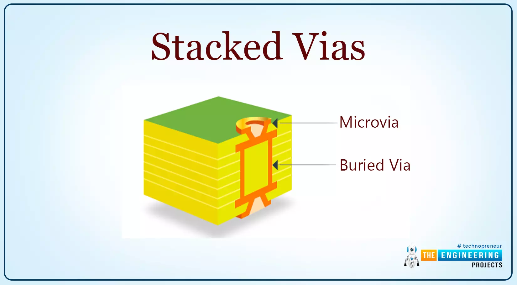
Stacked vias
This can be either buried or blind vias which have a very important function of connecting circuits between different layers of the printed circuit board and in this case across three or more circuit layers as shown in the figure below;
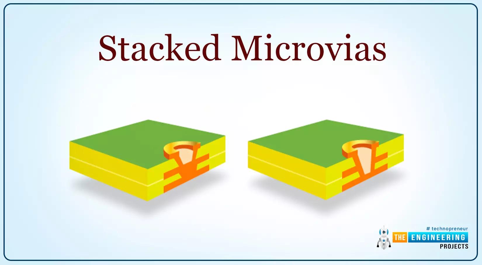
Stacked microvias
They can either be blind or buried but they are conical in shape. They are vert small and they still do the function of connecting circuits between layers of the PCB as shown in the figure below.
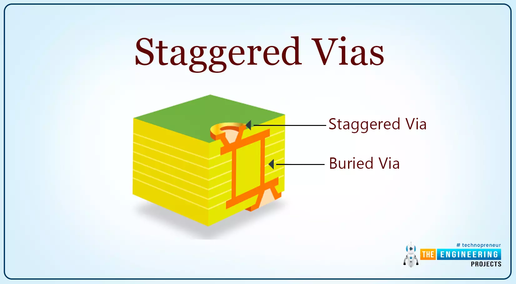
Staggered vias
When we have vias of a certain PCB layer connected without overlapping, they actually form a staggered via as shown in the figure below.
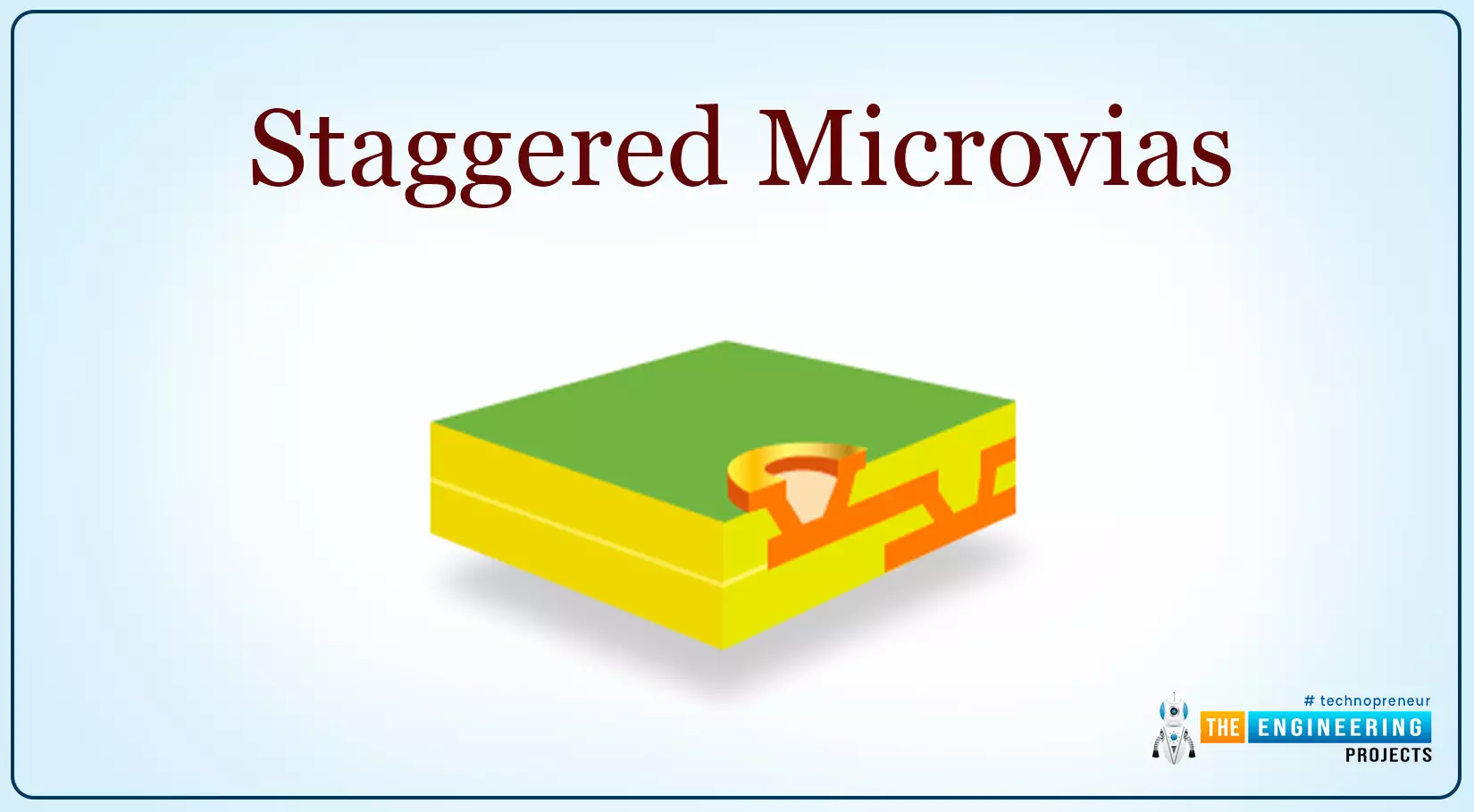
Staggered microvias
They are conical in shape but they are connected without overlapping hence forming a staggering structure as shown in the figure below;
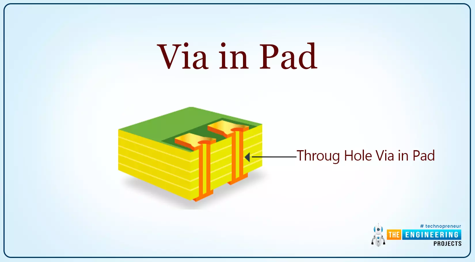
Via in Pad
This are vias that are connected to the pad where component is lied. They are very common in HDI PCBs.
HDI structure
There are mainly two structures that aren used in the manufacturing of the HDI;
- Buildup structure
- Any-layer structure
Buildup structure
This is the basic structure of the high-density interconnect PCB and uses the manual mechanical drilling as well as the laser drilling.
- The first step is the lamination of the core, it is drilled by the use of the mechanical drilling, platting is done before it is finally filled.
- Microvias are added to the core, followed by the drilling, filling and the whole process is repeated.
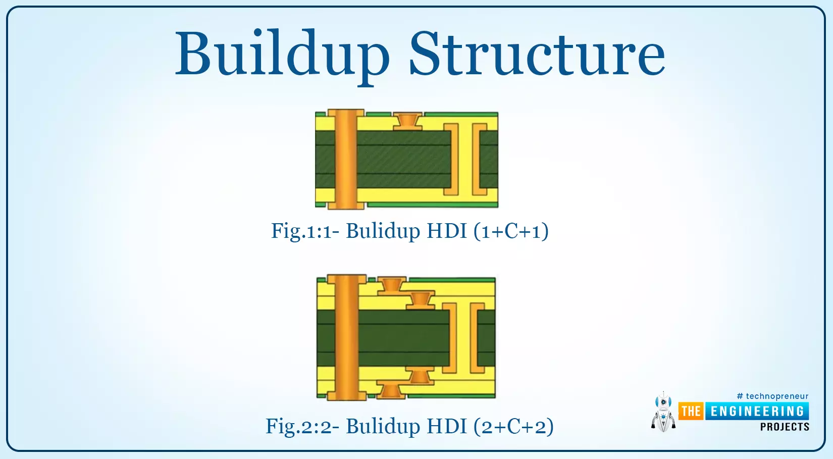
- The N- buildup structure is made up of the formular N+C+N where N and C represents the number of the microvia in each side of the core and the core respectively.
- The figures below shows an example of the N-buildup structures using the 1-buildup and the 2-Buildup
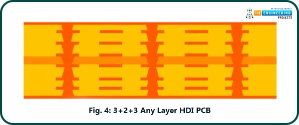
Any layer interconnect technology
This is an advanced technology that is used in the manufacturing of the HDI PCBs. The method is highly preserved for the high-level interconnection use since we can make connection of any of the two layers of the PCB without any form of restrictions. This means that any-layer connection has a lot of flexibility when it comes to doing these connections.
- Because there is no any restriction on how the connections should be made, this leads to the saving of the board spacing to about 30%.
- However, the cost of doing this board is higher and this is due to the complexity regarding the technology involved.
- Unlike what was done in the buildup, here the micro-via is drilled first by the use of the laser drilling, followed by the repeated copper platting process, transfer and pressing of the inner image, and finally transferring of the outer layer imaging.
- The figure below is a simple demonstration of the simple any-layer manufacturing process.
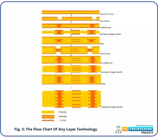
- The drilling process is done by the use of the carbon dioxide laser drilling machine
- The micro-via are made by the copper filling technology which will do the coper filling by the process known as the vertical continuous platting line and the horizontal plate line.
Benefits of the HDI printed circuit boards.
This technology has found great importance in the smartphone and the tablet manufacturing. Apart from that, they have become of great use in the laptops and desktop computers. The following id the great benefits of the HDI PCBs;
- Tighter designs; when we have a look at the high density interconnect PCB, we will realize that the board has very high intensity nature of circuit network connection. This high intensity implies that, the board takes literally less physical space. Utilization of design features such as blind and buried vias enables the designers to come up with more compact builds and this will make the HDI circuits very versatile.
- Reliability; the connectivity that is employed in the design of the HDI boards such as the use of the blind vias and the buried vias makes them more physical reliable. This is because such types of connection are less likely to get compromised.
- Lighter material; the material used is very light and cooler. The traditional and other PCBs use different variety of materials but the common one is the combination of copper, aluminium, fiber glass and other metals which might prove to be bulk. This is not the case with the HDI boards.
- Sharper signals; since these types of the PCB has more compact systems, then the outcome is that the signals will have a very short distance to travel hence avoiding much disturbances that comes in with the long-distance travel. This advantage makes the signal rich their destination undisturbed hence sharper performance of the board.
- Pocket friendly; four layers of the HDI boards are enough to perform all the functions of the standard PCB layer. The board having reduced size, it implies reduction in the coast too.
- Low power consumption; these types of boards have high number of transistors and also signals travel a very short distance. These features play a greater role in reduced power consumption in these types of boards.
Common uses of the HDI boards.
These types of boards have found many areas of use in the modern world of technology. Let us have a look at a few areas where the high-density interconnect boards are used;
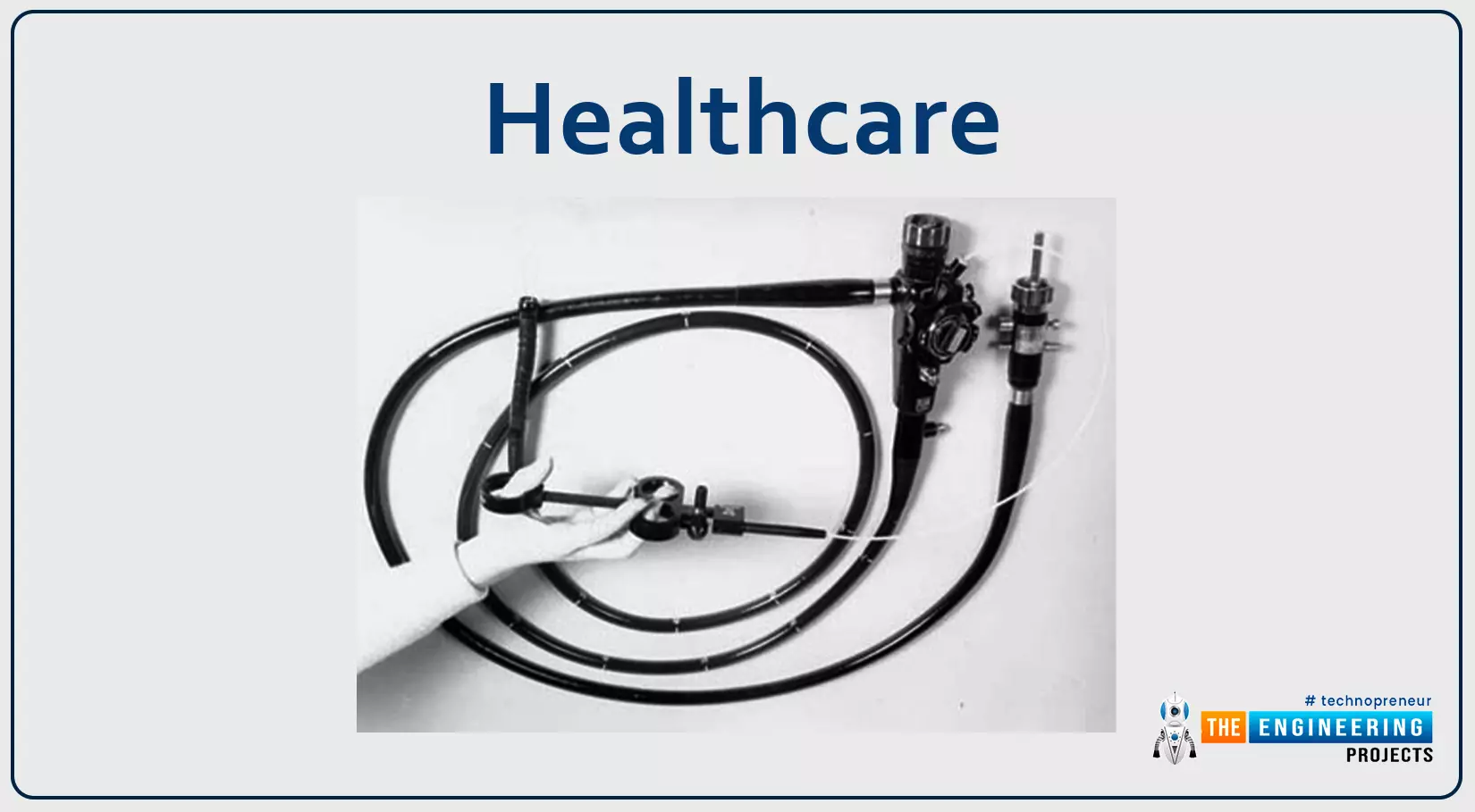
Healthcare
Due to the smaller size of the HDI boars, medical designers have found great interest in this type of board. The medicals equipment are compatible with HDI because they are very small and can fit into them for example in implants and also in the imaging equipment. The equipment play a very significant role in the treatment of the ailments and therefore smaller chips that require less intervention have to be used. Let us take an example of a heart pacemaker that is implanted in the heart to regulate the speed of the heart bit. The pacemaker should be very tiny and therefore the HDI has provided boards that can solve the size of the pacemaker issue. another good example is the colonoscopy which is passed through the colon of a human to carry out the colon examination. It is evident through research that so many people avoid the colonoscopy examination due to the painful experience but the availability of the HDI technology has drastically reduced the size of the camera and improved the visual quality of the same camera which has made the colonoscopy process less painful hence triggering the increased number of people searching for the service.
Aerospace and military.
Military use strategic equipment such as the missile and some other defense communication devices. This equipment utilizes the HDI technology in their boards since it is the only efficient available method. there have been greater changes in the aerospace technology and HDI have always provide the need solution. Communication devices such as the wireless pones and trackers are becoming very tiny in size and this is due to the involvement of too many tiny layers of the HDI boards.
Automotive industry.
The car and other automotive manufacturers are falling in love with the HDI boards simply because with this type of board you are assured of greater discoveries and innovations. This boards allows the saving of more space in the vehicle and also have an increased performance of the same vehicle. To be specific, Tesla uses the HDI technology to run the electric car system where it helps in extending the battery life of the system. Other driver assistants such as cameras, tables etc fit on the dashboard without much problems.

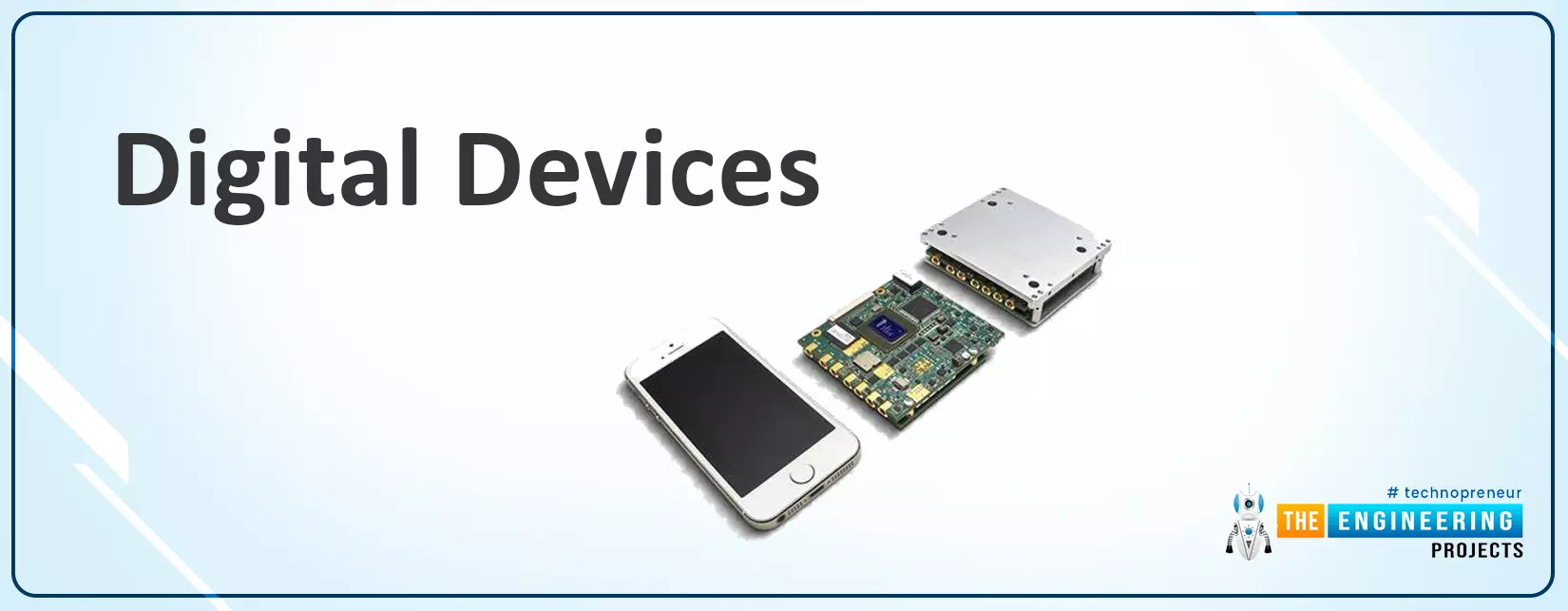
Digital devices.
Let us make a comparison of todays digital devices like the smartphone with what we had 10 years ago and you will make note that there is a very big improvement in size, thickness and weight. This has been made possible by the use of the HDI boards in this area. Thinner and more compatible smartwatches are also a product of the HDI boards.
Advantages of the HDI PCBs
- Compact design; the strategic use of the burred and blind microvias makes the board compact and this leads to spacing.
- High reliability; the preferred use of the stacked vias makes the board to have a super shield against the harsh environmental conditions.
- Phenomenal versatility; this board is ideal where weight, size and the performance are of great consideration.
- Cost effective; the functionality of a 6- layer standard PCB can be reduced to 4-layer HDI board without altering on its intended purpose.
- Better signal integrity; vias and pads and blind technology is what is mostly used in the HDI. It also has very short compact trucks or traces and this reduces the chance of the signals being interfered by the external forces hence achieving of very high signal integrity.