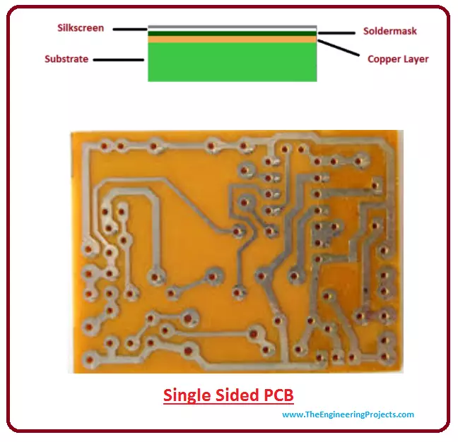
Introduction to Double-sided PCB


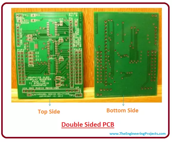
Hey Fellas! I hope you are enjoying your life. Today, I am going to share the 3rd chapter in the PCB learning series. In the last tutorial, we discussed Single-sided PCB in detail and today, we will have a look at the double-sided PCB. In double-sided PCB, the conductive copper layer is present on both sides of the board, unlike single-sided PCB where we have a conductive layer on a single side of the PCB. Thus, we can place electronic components on both sides of the double-sided board and normally use SMD components.
Let's jump in and explore more about double-sided PCB:
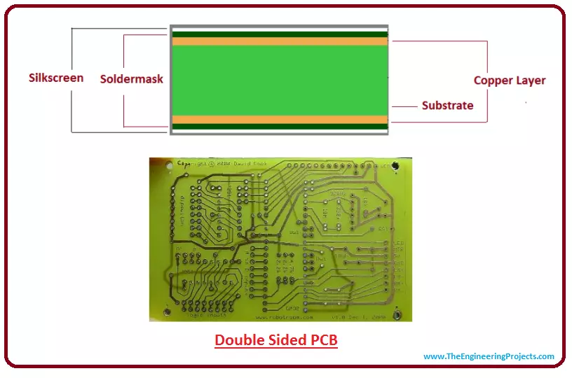
Double Sided PCB
- Double Sided PCB is a type of PCB that has conductive copper layers on both sides of the board.
- Simply put, double-sided PCB comes with two-sided traces or paths i.e. top layer and bottom layer.
- It is extremely useful in advanced electronic applications because of its small size and low cost as compared to multilayer PCB.
- Components on these boards can be connected using two different technologies i.e. Through Hole Technology and Surface Mount Technology.
- Double-sided PCBs are widely used in electronic industries ranging from intermediate to complex circuitry.
- They have become important in recent products because they permit closer routing traces compared to single-sided PCB.
- There are some examples where PCB comes with traces on both sides but components are connected only to one side of the board. Some people get confused if we still call it double-sided PCB if components are available only on one side of the board. But we still call it double-sided PCB even if components appear only on one side of the board because traces are present on both sides of the board.
- Soldering double-sided PCB boards is quite a tedious task, thus a pick-and-place PCB machine is normally used to solder these boards. We can't design these boards at home.
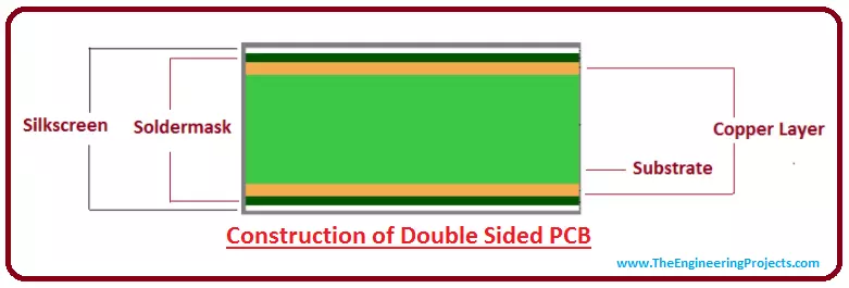
Construction of Double Sided PCB
- Construction of double-sided PCB is similar to single-sided PCB with some exceptions i.e. some layers are laminated on both sides of the board.
- The base of a double-sided PCB is composed of insulating material also known as a substrate which is mainly fiberglass/epoxy resin. What type of base material is used, defines if PCB board is Flexible PCB or Rigid PCB.
- Copper foil is laminated on both sides of the substrate in case of double-sided PCB.
- Similarly, the solder mask lies above the copper foil on both sides of the board.
- There exists a silk screen above the solder mask on both sides of the board, which is mainly used for adding symbols and characters on the board so a common person can understand the board's functions.
- All these layers that are used in the construction of double-sided PCB are the same as that of single-sided PCB, but these layers are appeared on both sides of the board as compared to single-sided PCB where these layers are present only on a single side.
Advantage of Double-Sided PCB
- Double-sided PCB is an ideal choice for most professionals because of its flexibility and ease of use.
- It comes with high circuit density and pertains to lower cost as compared to multilayer complex PCBs.
- Double-sided PCB can be developed using reduced board size which ultimately helps in reducing overall cost.
- If you intend to sink or source current or in other words, if your board provides current to other shields or slaves, then picking a double-sided PCB makes sense. You can use the bottom layer as a ground source.
- Double-sided boards have a leg over single-sided boards in terms of their complexity because if your board is densely populated and you intend to connect a lot of components on a single board then it is better to have some components connected on the bottom side of the board.
- If you are not allowed to change board size that can limit putting thicker traces, and you are instructed to route Vcc and GND on a single board, then it is better to pick a double-sided board and route Vcc and GND on the bottom layer.
Applications
Double-sided PCBs feature a moderate level of complexity and are mostly used in a wide range of applications and deemed useful where single-layer or multiplayer PCB fails to fulfill the requirement of the project. Following are some useful applications, this is just a glimpse of applications double-sided PCBs are used for.- Converters
- Control relays
- Power conversion
- HVAC
- LED lighting
- Instrumentation
- Industrial controls
- Power supplies
- Regulators
- UPS power system
- Traffic control system
- PC hard drives
- Vending machines
- Line reactors
- Test and monitoring equipment
- Printers
- Phone systems
- Automotive dashboards
- Power amplifiers
That's all for today. Now we have covered both single-sided and double-sided PCB. In the next lecture, we will discuss the detailed Introduction to PCB assembly. I hope you have enjoyed this article. I have tried my best to guide you with the most relevant and useful information that resonates with your needs and expectations. However, if still you feel skeptical or have any questions, you can ask me in the comment section below. I'd love to help you according to the best of my expertise. Thanks for reading the article. We feel happy when you guide us through your feedback and suggestions. They allow us to give your quality. Stay Tuned!