Manufacturing Process of Multilayer PCB


Hello! Readers, I hope you are pretty good. I am here with a new article to enhance your knowledge about advanced technologies. Today, we will have a detailed overview of the Manufacturing Process of Multilayer PCB. First, we will have a look at its basic definition, why there Is a need for this new type of PCB in presence of single layer and double layer PCBs. What are the merits and demerits of multilayer PCBs and pedagogy behind the construction process of these PCBs? Let’s start to take in all information about these PCBs. I try my best to deliver all of my research capacity for doing this job.
Introduction to Multi-layer PCBs
As to the name, it's clear that multi-layer PCBs are those which have several conductive layers over substantial material which is knowns as substrate. Unlike single layer and double layer PCBs which consist of one and two copper foil layers respectively, multilayer PCBs contain more than three lays on a single board.
Before discussing the multi-layer PCBs let put a throwback to What’s PCB. How are they classified and what are they used?
Printed circuit board (PCB)
The word PCB comes from a printed circuit board that consists of sleeky copper chips on it which are conductive. These tracks are linked with each other electrically.
How to Manufacture Multilayer PCB?
In order to manufacture a PCB board, you need to take the help of a PCB Fabrication company. There are many online PCB companies available. where you can place your PCB order on their official website. While placing your order, you need to select all your specifications/requirements and they will give you the cost and time to complete it. Let's place an order of Multilayer PCBs on PCBWay Fabrication House. PCBWay is a well-renowned PCB Fabrication house, provides excellent prices and discounts on first orders. Moreover, they have an excellent support team, ready to help you, 24/7. So, let's place our PCB order:
- First of all, open the official site of PCBWay(PCB Manufacturing House).
- Now, at the top, you will find an instant quote screen, click on the button to open the PCB Calculator page, as shown in the below figure:

- As you can see in the above figure, I have placed an order for a multilayer PCB having 4 layers.
- I have added a size of 100x100mm and have placed an order for 10 pcs of PCB.
- PCBWay has given me a cost of $139 for standard manufacturing and with shipping in America, the total cost is $166.
That's how easy, you can place a manufacturing order for PCB.
Criteria for classification of multi-layer PCBs
There are many ways by which we can categorize different types of PCB. Most commonly they are classified on basis of their layers , types of substructure material , conductive layers and rigidness of the boards, etc. Now put a little thought into describing these methods.
- Number of layers
- Type of base substantial
- Thickness of conductive layer
- Rigidness
Number of layers
This methodology divides PCBs into single-layer PCB , double-layer PCB, and multi-layer PCB . if PCB has a computerized structure on one side then it terms a single layer PCB. if they have a circuit on both sides of the board then it is termed as double-layer PCB but with the invention of technology and with the enhancement of our need we require complex electronic structures which take less space but do more than one task on a single device. Due to which we mounted more than two layers over a single board to form a multi-layer PCB. It has more layers and flexibility than two earlier PCBs which are single layer PCB and double layer PCB. Under the present rank of technology, we can form PCB having almost 32 layers.
Type of base substantial
The material which is mostly used in the preparation of PCBs is fiberglass, cyanate ester, polyamide, and polyester reinforcement. The substantially material should be
- Dimensionally stable under heating process
- Have good strength of attachment with another conductive layer
- Beneficial in electrical impedance
- Highly elastic
The thickness of the conductive layer
This method sort out the PCBs on the basics of consistency of copper foil and the breadth of conductor route onboard. The board ness of a copper layer may alter from 0.0014 to 0.0042. These factor combined determines the cross-sectional area of the board. Which in return decides how much current can a conductor carry.
Rigidness
For offering the reinforcement to the circuit which must have an electrical connection between them we require a rigid PCB. To furnish the rigidity, the thickness of the board must be almost 1.6mm. variety of substantial materials are used for this purpose.
Kinds of PCB
There are three kinds of PCB as given below
- Single layer PCB
- Double-layer PCB
- Multilayer PCB
Overview to multi-layer PCB
- If you are focus on the name of this PCB which is Multilayer it clear that it is a type of PCB which have more than two layers. In simple Words multilayer PCB have several conductive layers on a single board.
- They are favored in many elegant industrial tasks and motherboards etc.
- Most importantly where we need to save space we can use these PCBs for example in a digital camera, android mobiles even on compact disk.
- Multi-layer PCBs which are available now a day in markets have 4 to 8 layers.
Construction of multi-layer PCB
- Multi-layer PCBs area unit designed by connecting all the quantity of lays and material at heat and pressure therefore on take away any at bay air between layers.
- Organic compounds and staff are employed to stay the parts and different lays along.
- You have a choice in choosing a variety of materials like exotic ceramic, epoxy glass, Teflon, etc. to fabricate the PCB.
- The various prepreg and core layers area units combined and bear the lamination methodology happening at heat and pressure that helps to moderate the layer along. Later on, the PCB is cooled then it becomes rigid and solid board.
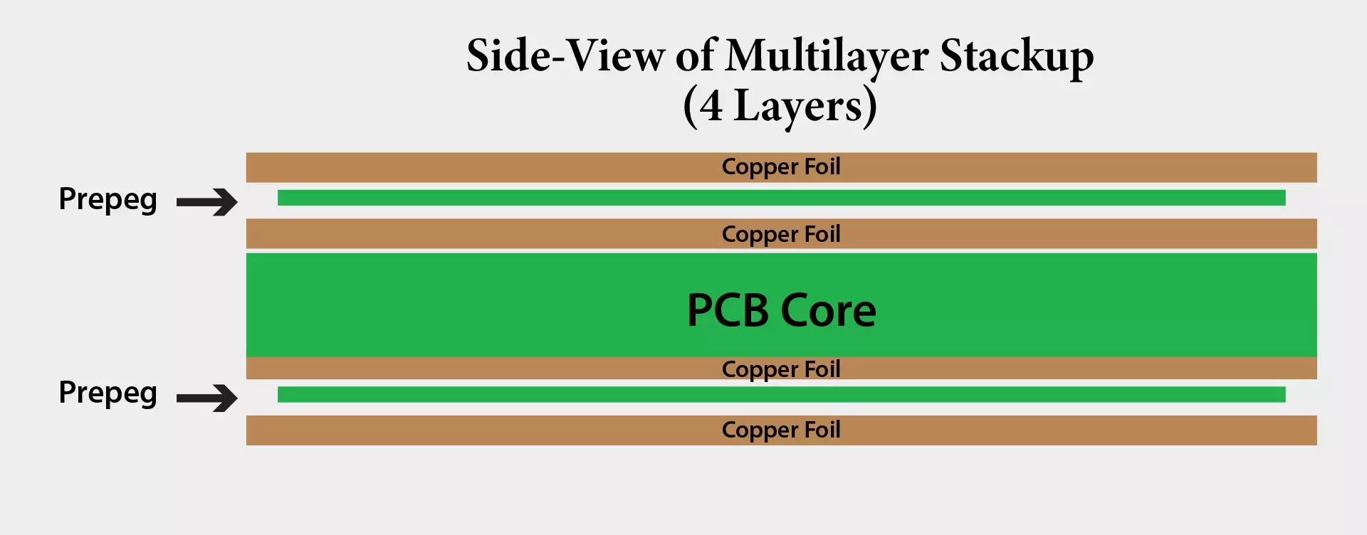
- The internal layers of multi-layer PCBs consist of special material which is known as prepreg.
What is prepreg?
- The lays of the healed panel in multi-layer PCB are freestanding by a sheet of B stage organic compound, which is termed prepreg. This layer aims to adhere to the rigid layer with each other and fixing the board between layers.
Problems faced by experts in manufacturing multi-layer PCBs
One biggest issue faced by manufactures while dealing with fabrication of multi-layer PCBs is drilling hole technology.

Technique for interconnecting layers on MLBS
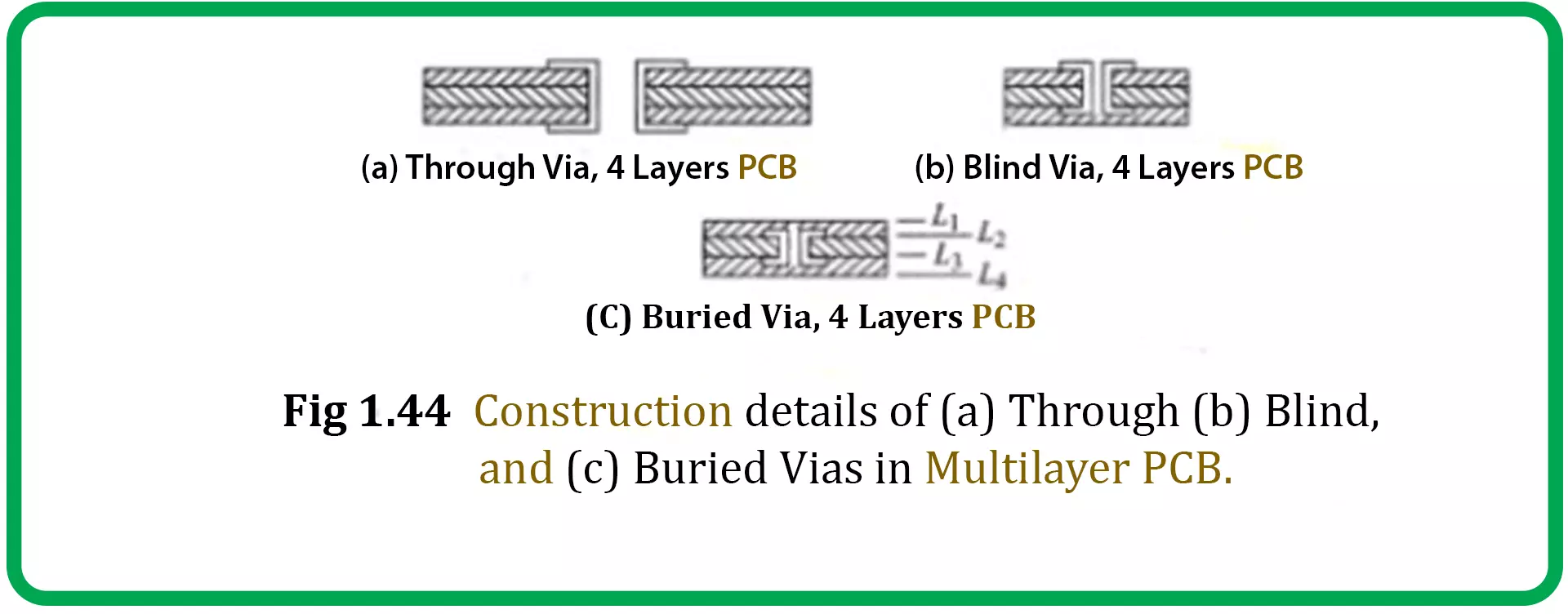
We can make an electrical connection between components which present on several layers of multilayer PCB by using different methodologies which we are given below ;
- Through-hole via
- Through buried via
- Through blind via
What is via?
As we discuss in the previous article VIA is a vertical hole on board that is then filled with metal foil for interconnecting the component. Different modes of via to tackle this situation are elaborated below ;
Through-hole via
By using this technique we can join components of the upper side of multilayer PCBs
Through buried via
By using this pedagogy we can link the internal lays of multi-layer PCBs.
Through blind via
A blind via can link the topmost layer with internal layers of multilayer PCB.
Lamination method of multi-layer PCBs
- Internal layer gist, coating of B stage resins, and coating of atomic number 29 foil are used in the lamination process of multi-layer PCBs.
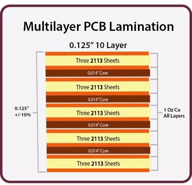
- Drilling of holes in the coating of substrate and core is utilized to line up them as they are stack aboard.
- For a four-layer PCB, we require a sheet of foil and a suitable range of woven glass cloth with epoxy resin.
- The stack of the panel is fabricated on a meaningful conductive plate and once it’s completed the plate becomes a valuable board.
- Now we heat this board under necessary conditions.
- The application of pressure, heat, and vacuum on board forced the organic compound to become flexible and consistent across core and foil surfaces.
Why do we need multi-layer PCB?
Here we discuss under which situation we preferred multilayer PCB over the other two.
- To tackle problems related to weight and volume which are commonly seen by experts during their works multi-layer PCB Is their solution.
- For a composite electrical circuit, multilayer PCBs are less pricy than a single layer and double layer PCB.
- Multilayer PCBs are help full in reducing the resistance problems in an electrical circuit and increase the chances of supply of current which in return increase the flexibility and demand of products.
- It increases the reliability of electrical circuits
- For a circuit that requires several numbers of interconnection multilayer PCBs are ideal. They allow high-speed performance.
Common mistakes in the manufacturing process of multi-layer PCBs
- Irregularities of electrical connections onboard are the biggest problem by which ones have to tackle.
- Delay between layers during bonding causes poor care in bonding. Other puzzling circumstances are discussed below.
- High resistance causes a big issue due to poor plating in holes.
- Inadequate tooling techniques.
- Due to high stuff of components into small available space causes an uninventive structure.
Key points to overcome these problems
To get better-fabricated multi-layer PCBs one should follow these steps
- The developer must be highly experienced and he must concentrate their attention on quality.
- He must have the strength to control the process.
- The board must be stocked in a bit of time and dried for almost 120 minutes at 120°C.
Advantages of multi-layer PCBs
There are many merits of multi-layer PCBs. Let’s start to grasp the knowledge about advanced technology rewards.
- We can tackle many problems at a time by using multi-layer PCBs.
- It offers less resistance and enhances power distribution between electric components on board.
- Multi-layer PCBs are less weight and have a small size which has adorable uses in advanced technology which becomes handy with time.
With the aid of multi-layer PCBs, we can have boards which although are small in size but are more compatible to tackle problems.
- Multi-layer PCBs are favored for the high-speed circuitry process.
- Multi-layer PCBs decreased the chance of EMI expelling which comes due to small loop area and high distributed capacitance.
- Multi-layer PCBs are highly persistent as they are configured at a High level.
- With the increments of layers in a single structure trim the size and become compatible to link more electronic components in the available space.
- Multi-layer PCBs are designed by high standardized fellowship therefore multi-layer PCBs are prefabricated.
Disadvantages of Multi-layer PCBs
As we know that there is some raw fact about everything. Multi-layer PCBs also have a demerit. The weakened point of multi-layer PCBs are discussed below;
- Multilayer PCBs require High expenditure. The manufacturing process of Multi-layer PCBs requires a heavy budget.
- Although multi-layer PCBs are very worthy due to their small size in advanced technology at the same time, It is not an easy task to tackle with an intensive circuit on a single board. A very careful mental focus is required while working with multi-layer PCBs.
- It is difficult to mend and retread the interconnection of multi-layer PCBs.
Applications of Multi-layer PCBs
Multi-layer PCBs have outstanding features. This worthy characteristic makes it popular for usage. Multi-layer PCBs have applications in household appliances, industrial works, wireless computing, ballistic capsule, and many other instrumentations. Multi-layer PCBs have distinguishing characteristics in the development of vast practical applications. Some applications of Multi-layer PCBs are illustrating below;
- Because of their small size, multi-layer PCBs are utilized in handy technologies like android mobiles, cameras, motherboards.
- Multilayer PCBs are used in signal transmission which requires more accuracy in processing.
- Multilayer PCBs are used in navigational computing.
- Multi-layer PCBs are used in holding the data safely.
- Multilayer PCBs are used in communicating technologies. The use of multilayer PCBs trims the size of new inventions.
- Multi-layers PCBs are used in challenging situations for the trial process of different instrumentations.
- For forecasting atmospheric conditions multi-layer PCBs are used.
- Multi-layers PCBs are used in the instrument which is utilized for observing the cardiac conditions.
- Multi-layers PCBs are Second hand in warning devices.
- Multi-layer PCBs play an important role in the fabrication of robotic space Vehicles designed to voyage the earth's orbit.
- Multi-layer PCBs are used in computed axial tomography scanners helpful to an analyzed brain tumor.
- Multilayer PCBs are used in roentgen ray instrumentations. These instruments tackle medical problems.
- Multi-layer PCBs are used in industrial systems for controlling purposes.
- Multi-layer PCBs are specifically worthy in technology associated with satellites, missiles, aircraft, and spacecraft.
- Even we can say that the building block of innovative conception is multi-layer PCBs. It becomes the need of fast, durable, flexible and valuable designs.
Conclusion
In the end, we conclude that there are more number layers in multi-layer PCBs than single and double-layer PCBs. Multi-layer PCBs have Unmatched properties, valuable applications but in the end, nothing is perfect each technology has some drawbacks like this multi-layer PCBs also have some drawbacks.
In modern computing, the demand for multi-layer PCBs is more than the other two PCBs.- You always need to opt for which kind of PCB you would like.
That’s all for today’s article. I hope you've got enjoyed the article and build a grip on the understanding points. However, if you continue to face any skepticism concerning multi-layer PCB then please be at liberty to depart your queries within the comment section. I'll give a solution to those inquiries to the simplest of my data and researching skills. Also, give North American country along with your innovative feedbacks and suggestions you improve the standard of our work and supply you content in keeping with your wants and expectations. keep tuned! thanks for reading this text.