A Detailed Guide on PCB Manufacturing Process


Hi Friends! I welcome you on board. Happy to see you around. In this post today, I’ll document a detailed guide on the PCB manufacturing process.
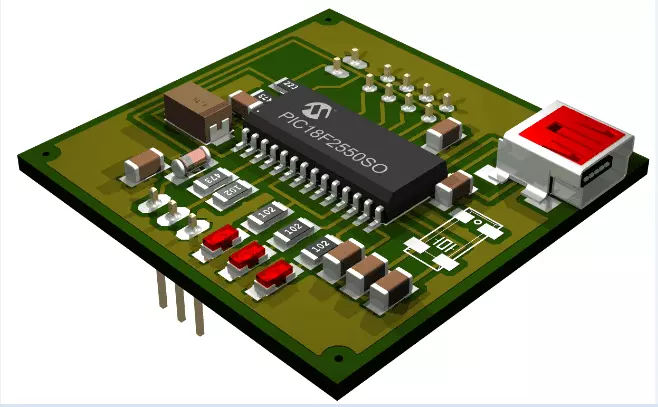
PCB is hands down a crucial part of modern electronics. From cell phones and digital clocks to remote control and television sets, you will find inside a printed circuit board that connects the electrical components through sophisticated layers of copper traces. These electrical copper traces help in the flow of current through the connected components.

Needless to say, PCB has revolutionized the electronics industry. You’ll never find bulky electronics incorporated with scores of wires and electrical components. Nowadays, electronic devices are more compact and sophisticated, cover less space, and are capable of doing more functions than their predecessors.
- If you don’t want to dive into the nuts and bolts of this hectic PCB manufacturing process, you can outsource your PCB design. There are many online PCB Companies i.e. NextPCB, PCBWay, etc. that help you design your PCB according to your projects' needs & requirements.
- You can simply submit your details, and they will create the PCB design customized to your exact requirements.
A Detailed Guide on PCB Manufacturing Process
Circuit boards are mainly categorized into three main types. And all these types are used in different applications.

You need to understand the main difference between all these types, so you can pick the right one based on your requirement.
Main Types of Printed Circuit Board
The following are the three main types of circuit boards.
Single-sided Circuit Boards
Single-sided PCB, also known as single layer PCB, is made with the rigid laminate of woven glass epoxy material which carries one layer of copper traces on one side of the board and another side is used to place the different component on the board. These electrical components are electrically connected through copper traces on the board.
Double-sided Circuit Boards
Double-sided PCB, also known as two-layer PCB, is composed of the same rigid laminate of woven glass epoxy material as single-sided PCB, but here in this case both sides of the board are covered with copper traces. And mainly based on the applications, these traces are made with varying thicknesses.
Multiple-sided Circuit Boards
Multiple-sided PCBs are similar to single-sided or double-sided boards, but here in this case copper foil is used instead of copper coating. The copper foil continues to make multiple layers until you get the desired number of layers.
Main Parts of PCB
Before we study the complete manufacturing process, let’s discuss the main parts of the printed circuit board.
Substrate
This is the skeleton of PCB – the most basic structure. Fiberglass is used to make the substrate. Fiberglass extends the core strength to the PCB and keeps the board from breakage.
Copper Layer
The next part is the copper layer. Based on the type of PCB, copper foil or copper coating is used on one side or both sides of PCB. The purpose of this copper trace is to provide an electrical signal between the connected components on the board.

This is similar to the brain nervous system where neurotransmitters are connected with the muscles to collect and provide information to the brain.
Solder Mask
The third part is the solder mask. It is a protective layer made of a polymer that acts as a PCB skin. It protects the copper layer and keeps it from short-circuiting.
Silkscreen
Silkscreen, also known as legend or nomenclature, is the final part of the PCB. It is normally laminated on the components side of the board. This layer is used to represent symbol switch settings, logos, part number, test points, and component reference.
PCB Manufacturing Process
Hope you understand the main parts of the PCB. Now, let’s dig deep into the manufacturing process.
Step 1: The Design
It all starts with the basic design. A detailed PCB design is made on the dedicated PCB design software or you can also use online PCB design services to design your PCB.
Commonly used PCB design software is Eagle, Altium Designer, Pads, OrCad, KiCad, or Proteus, etc
Once the design is finalized, the file is exported. Make sure… you export file in the format that the manufacturers support. The commonly used file format is known as extended Gerber. Know that… different software include different Gerber file generation steps, however, they all include detailed information about drill drawing, copper tracking layers, component notations apertures, and other options.
Step 2: The Print
The plotted printer is used to print PCB. It generates the resultant film which is composed of various layers. The blank ink represents the conductive copper traces while the clear ink indicates the non-conductive areas. This is the representation of the inner layers. In outer layers, this trend is reversed i.e. the clear ink indicates the conductive copper traces and black ink indicates the non-conductive areas.
Step 3: The Substrate
The substrate is the skeleton of the PCB that is composed of fiberglass. This is an insulating material that connects the various elements.
Step 4: The layers
In this step, a laminate is created using the blueprints. This laminate is then covered with the photo-sensitive film which is also called a resist. This resist is composed of photo-reactive chemicals which when exposed to UV light, hardens the resist.
Step 5: Hardening the Photoresist Layer
The next step involves the revealing of underlying copper pathways. This is done by hardening the photoresist layer.

When a combination of laminate and resist is sent to the room under UV light, it hardens the photoresist layer.
Step 6: Removing Unwanted Copper
This step involves the removal of unwanted copper. An alkaline solution is employed to get rid of unwanted copper. Make sure during this process, it doesn’t harm the photoresist layer.
Step 7: Inspection
In this step, layer alignment and optical inspection are carried out. The inner and outer layers are aligned by the holes. A punch machine is used to make sure everything is aligned and in place.
Step 8: Lamination Process
At step 8, inner and outer layers are pushed together for the lamination. These layers are fused together once they are inspected, making sure they are defect-free.
Epoxy resin known as Prepreg is used with the metal clamps to keep these layers in place. The layer of substrate and copper coil is placed over the Prepreg. A mechanical press is then used to punch everything together where specialized pins are used to keep each layer in place. The PCB layers are fused together in the presence of epoxy that melts down due to applied heat and pressure. The top press plate and pins are then removed to pull out the actual PCB.
Step 9: Drilling
After the lamination, there comes the drilling process. But before initiating the drilling process, drill spots are located using an X-ray machine.

A computer-guided drill is used to create holes. After the drilling process, additional leftover copper at the edges is removed.
Step 10: PCB Plating
Once the drilling step has been completed, a certain chemical is used to fuse all layers together. This process is known as PCB Plating.
The PCB layers are then thoroughly cleansed together in a series of chemicals. This bathing process applies the copper layer on the top of the layer and in between the drilled holes.
Step 11: Outer Layer Imaging
After PCB Plating has been completed, another layer of photoresist is applied to the outer layers of the design. Which gets harden in the presence of UV light.
After coating the outer layers with photoresist, they are again fused together in the presence of certain chemicals like we did for inner layers in the previous PCB plating step. Though the plating process is the same as the previous step, the outer layers develop the plating of tin, thus guarding the copper of the outside layer.
Step 12: The Last Etching
The tin guard developed in the last out layer imaging is used to protect the copper layer during the etching of the outside layer. The same copper solvent is used to remove the unwanted copper while the tin guard continues to protect the copper of the outside layer.
Step 13: Applying the Solder Mask
The proper PCB connections have been developed once the unwanted copper is removed. Now comes the solder masking. The final panels are cleaned before applying the solder mask. Once the cleansing is done, solder mask film is applied with ink epoxy.
The final product is then exposed to UV light to remove the unwanted solder mask. After the removal of the unwanted solder mask, the PCB is heated in the oven that cures the solder mask and results in the green color of the PCB panels.
Step 14: Final Surface Finish
The final surface finish is achieved by the plating of materials like silver and gold. This surface finish results in developing the core strength and improves the bonding of the elements.

Once the plating with gold and silver is achieved, the resulting product is then silkscreened. The necessary information including company ID numbers, manufacturer marks, and warning labels have been printed on the PCB during this silk screening process.
Step 15: Electrical Testing
Once the final surface finish has been completed, the entire PCB goes through a series of electrical tests to ensure functionality.
These electrical tests include isolation and circuit continuity tests. The isolation tests scan the isolation values of PCB to ensure if there is any short circuit. While the circuit continuity test confirms if there are any disconnections in any area of the board. These tests not only confirm the board’s functionality but also how the initial PCB design is observed during this manufacturing process.
Moreover, these tests can be applied both ways: in the automated environment or under the supervision of a practiced technician.
- If you don’t want to dive into the nuts and bolts of this hectic PCB manufacturing process, you can outsource your PCB design. PCBWay Fabrication House helps you design your PCB for the required project.

- You can simply submit your details, and they will create the PCB design customized to your exact requirements.
Step 16: Final Cutting Step
Once the final product is run through a series of electrical tests, there comes a cutting process that results in removing and cutting the PCB from the original panel. You can cut PCBs from the original panel using V-groove or CNC machine.
Your final PCB product design is now ready that you can use in your electrical project.
That’s all for today. I hope you find this article helpful. If you’re unsure or have any questions, you can pop your query in the section below. I’d love to help you the best way I can. Feel free to share your valuable suggestions and feedback around the content we share so we keep sharing quality content customized to your exact needs and requirements. Thank you for reading the article.