


What is Multilayer PCB? Definition, Manufacturing & Applications


Hello Friends! I hope you all are well. Today, I am going to share the 15th lecture in the PCB learning series. I am going to give you a detailed overview of Multilayer PCB, we will cover what is Multilayer PCB? & why do we need to use it? We will also discuss its Construction, advantages, disadvantages, etc. We have seen single-sided PCB and double-sided PCB in our previous posts, so go through them first.
Let's first have a look at the definition of PCB:
- PCB is an abbreviation of the printed circuit board, which comes with different copper conductive paths, traces & pads, incorporated on a single board to electrically connect different electronic components.
So, let's get started with What is MultiLayer PCB?
What is Multilayer PCB?
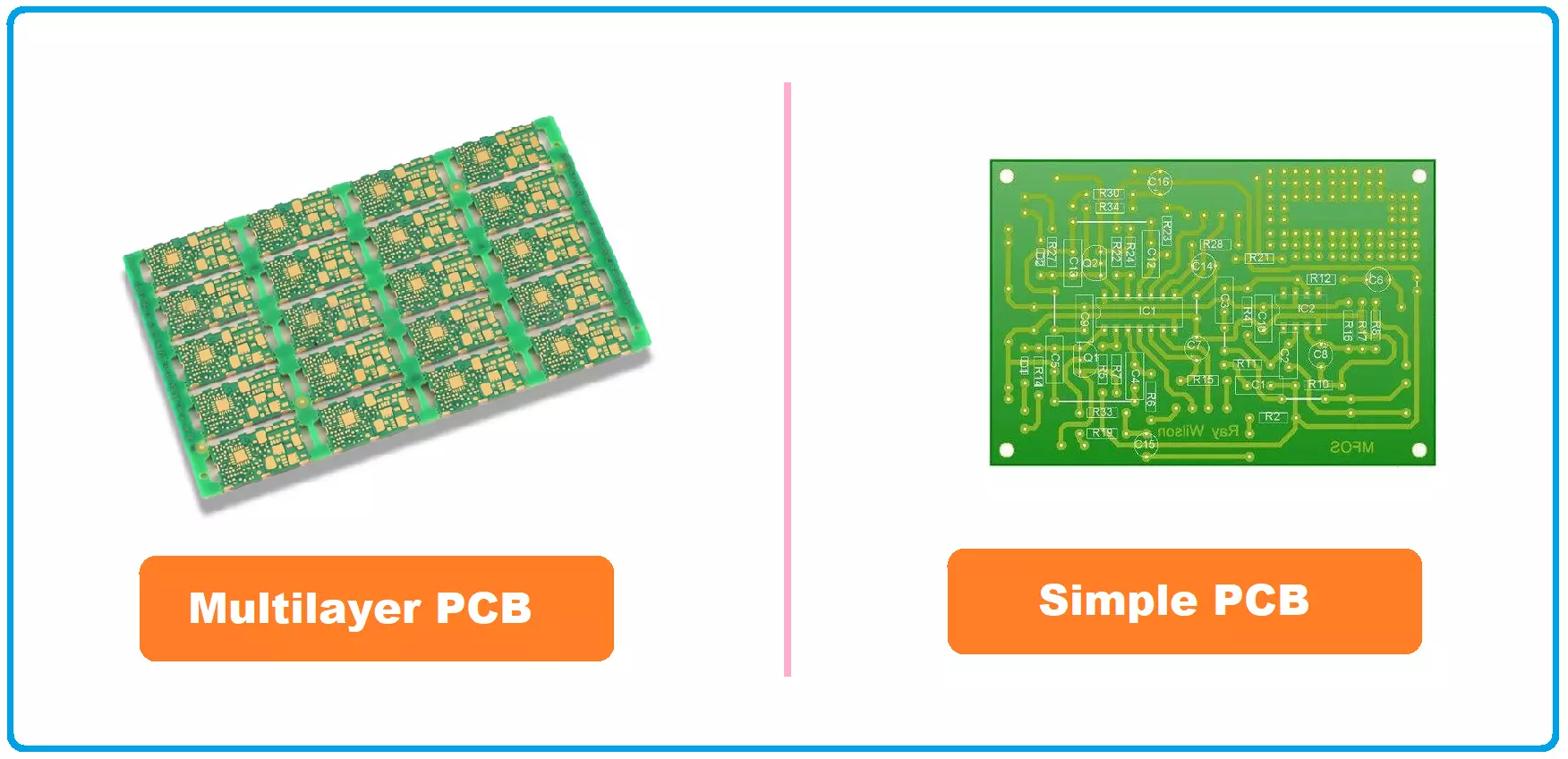
Initially, electronic components were available in DIP packages only and PCB boards were used to be large-sized, thus having more space for the PCB wirings/connections. But with the research in nanotechnology, electronics get introduced with SMD(Service Mount Device) components. SMD components are very small-sized components and their sole purpose is to reduce the overall size of electronic kits/circuits. So, now when SMD components are used in PCBs, they are placed very close to each other, and in complex designs, there's not enough space to pass the tracing lines of connection wires. So, to overcome this issue, Multilayer PCBs are introduced, where connections/wirings are split across different PCB boards(called layers) and these layers are laminated to keep them insulated from each other and glued together. So, any PCB having 3 or more layers is termed a MultiLayer PCB .
Multilayer PCB Definition
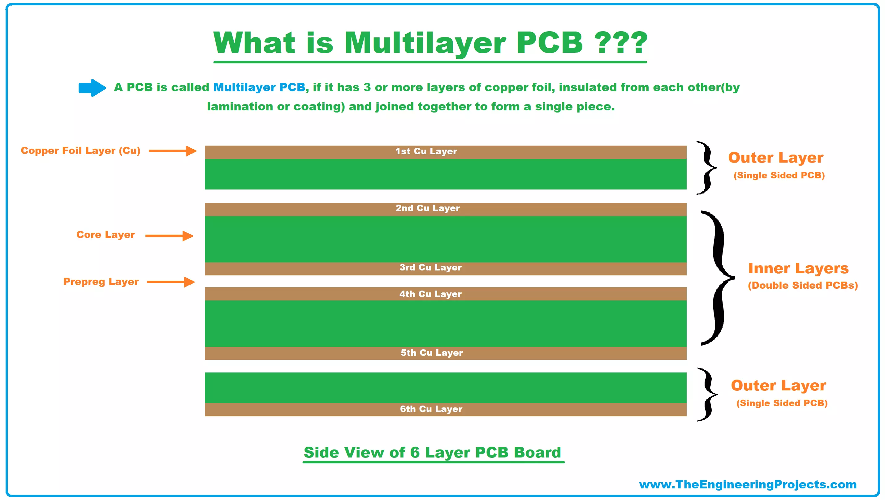
- A PCB is called Multilayer PCB, if it has 3 or more layers(sheets) of copper foil, insulated from each other(by lamination or coating) and joined together to form a single piece.
- A Multilayer PCB has an Inner Layer Core present at the center of all the layers and coated with a Copper layer from both sides, while layers of prepreg(woven glass cloth with epoxy resin) are used for insulation.
- In Multilayer PCB, outer layers(top & bottom) are single-sided PCBs , while the inner layers are double-sided PCBs .
- In multiplayer PCBs, few layers might be assigned with fixed tasks and are termed as planes i.e. power planes, ground planes .
- Layers in Multilayer PCB are normally connected with each other in 3 different styles, named as:
- Through-hole Via.
- Blind Via.
- Buried Via.
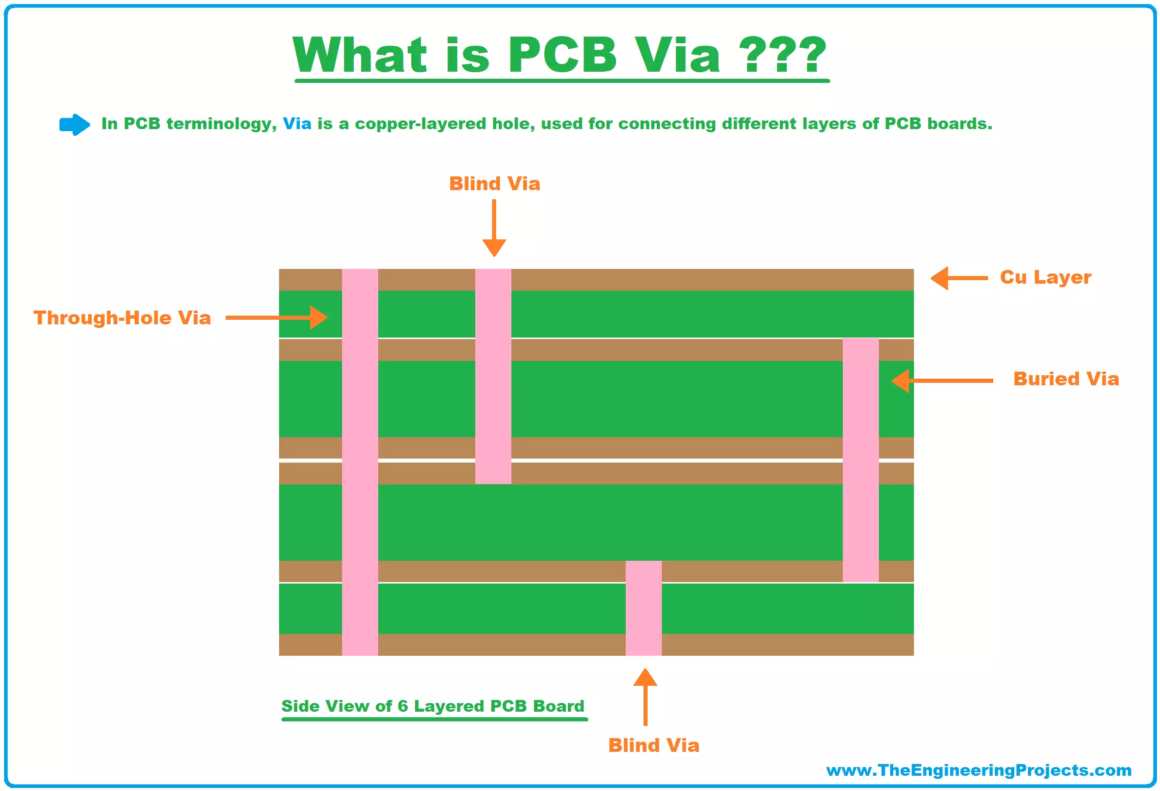
What is PCB Via?
- In PCB terminology, Via is a copper-layered hole, used for connecting different layers of Multilayer PCB.
- There are 3 different styles of Vias available, discussed as follows:
- Through-hole Via: This Via connects all layers of a multilayer PCB from top to bottom.
- Blind Via: This Via connects any outer layer(top or bottom) with one or more inner layers of Multilayer PCB.
- Buried Via: This Via connects any number of inner layers and never connects with any outer layer(top or bottom).
MultiLayer PCB Key Points
- Multilayer PCB is normally Rigid PCB because it's too difficult to design it in Flexible PCB format.
- Depending on projects' requirements, up to 100 layers can be incorporated in a single multilayer PCB.
- However, 4 to 8 layered PCBs are normally used for common electronics products, while some smartphones are equipped with 12 layered PCBs as well.
- Layers are tightly glued together in multilayer PCB, but if you look closely you can count layers on a single multilayer board.
- Multilayer PCBs are used on an industrial scale & nowadays every electronic product is equipped with multilayer PCB(could be multiple).
- If you check the electronic circuitry of any modern home appliance i.e. Smart LED, Mobile Phone, Laptops, etc. , you will find multilayered PCBs everywhere.
- If you are planning to design PCB online, you should have a look at these Top Online PCB Design Services .
Why do we need MultiLayer PCB?
Electronics have evolved rapidly in the past few decades. In the 1990s , mobile phones were used only to make calls or receive msgs but today, we have literally incorporated a complete computer in these small mobile devices and it won't be possible without using Multilayer PCBs. Multilayer PCB with SMD components brings smartness to electronic products by making them small-sized and thus handier. The modern world is trending towards miniaturization and multilayer PCB is playing the role of a backbone. Multilayer PCB design plays an important role in determining the functional and thermal performance of the complete electronic system, and as multilayer PCB is designed in PCB industries under modern PCB machines, thus it fulfills all standards and is durable as compared to simple PCB boards. Advanced electronic products use multilayer PCB because it allows a large number of components to incorporate on a single board, hence allowing the higher components density.Multilayer PCB Manufacturing Process
Now let's have a look at How to Manufacture a Multilayer PCB from scratch. It involves the following steps: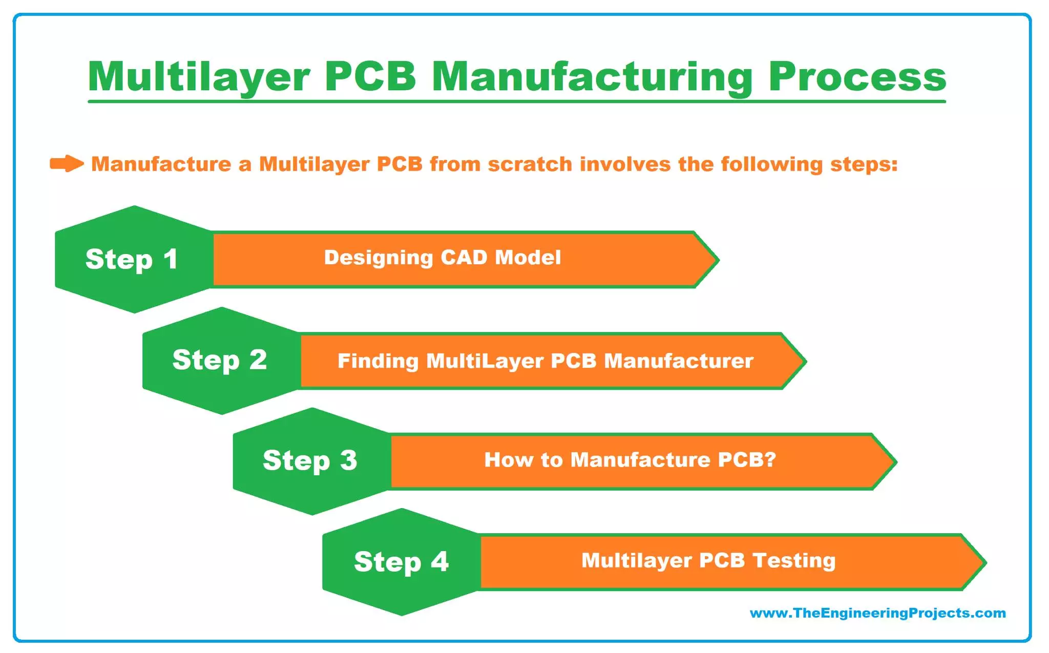
Step 1: Designing CAD Model
- The first step involves the designing of the software model of Multilayer PCB .
- PCB Designing Tools i.e. Altium, Proteus, etc. are used for designing the PCB layout.
- As Multilayer PCB designs are complex so expert & professional designers are required.
Step 2: Finding MultiLayer PCB Manufacturer
- It's the most important step as different PCB manufacturers are available online offering different prices & qualities.
- Few important things to check during the selection process are:
- Maximum number of Layers.
- Via styles.
- Layers thickness.
- Drill sizes.
Step 3: How to Manufacture PCB?
- The PCB designer's task has been completed, as Multilevel PCBs are manufactured by PCB companies i.e. JLCPCB, PCBWay, etc.
- In order to manufacture multilayer PCB, prepreg & core materials are joined together and are subjected to high temperature & pressure to remove any trapped air between the layers.
- Resin is used to cover the conductors around the corners, while adhesive material is melted under nominal temperature to stick different layers together.
- You can pick your material from a number of different combinations i.e. exotic ceramic, epoxy glass, or Teflon.
- It takes around 2 hours to cool off the material and will result in a hard and solid multilayer PCB board.
Step 4: Multilayer PCB Testing
- Once PCB Manufacturing company completes the product, it will ship the PCB order to the mailing address.
- Now the designer needs to unpack it and plug it in the testing workbench.
- Flexible connectors are normally used to interface Multilayer PCBs with other devices or PCBs.
Advantages of Multilayer PCB
The demand for Multilayer PCB is growing exponentially in electronics products. Multilayer PCB has numerous benefits when it comes to electronics circuit designs. Let's have a look at few advantages of Multilayer PCB: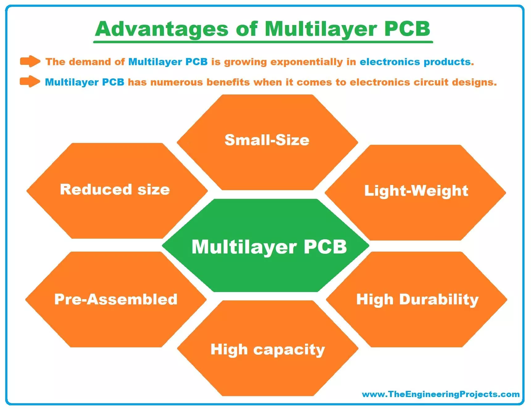
1. Small-Size
- The main & foremost advantage of Multilayer PCB is its small size .
- Electronics Gadgets(i.e. smartphones, LCDs, microwave ovens, etc.) are updating their models and becoming slim & compact by increasing the layers of their PCBs.
- Old mobile phones(20th century) normally used 4 to 8 layered PCBs while modern mobiles are using up to 12 layered PCBs.
2. Light-Weight
- As Multilayer PCBs are small-sized and SMD components are placed on them, so they normally have very low weight .
- Because of this lightweight feature, multilayer PCBs are used in hand-held electronics devices i.e. medical devices(Heat Beat Monitors, Blood Pressure Monitors, etc.), mobile phones, electronic watches, etc.
3. High Durability
- As Multilayers PCBs are designed on a professional level, thus Multilayer PCB manufacturing process is highly advanced & precise .
- As we discussed in the Multilayer PCB manufacturing process, these PCBs are designed under professional care with formulated ingredients, that's why multilayer PCBs are highly reliable and durable.
4. More Power in Small Package
- Because of multilayer PCB, electronics circuits get reduced in size, thus giving the opportunity to add more electronic components in the same space.
- The density of components(in the same space) can also be increased by increasing the layers of PCB.
- That's the reason why our mobile devices, graphics cards, etc. are becoming slim & powerful with time.
5. Pre-Assembled
- Multilayer PCBs are designed by professional PCB companies and the Multilayer PCB manufacturing process involves machining only.
- So, the user just needs to design the PCB layout(on software) and place the order on any Multilayer PCB manufacturing company and after that, it's the job of the PCB company to provide the final product.
Disadvantages of Multilayer PCB
There are many benefits of picking multilayer PCB, but it also comes with some disadvantages/drawbacks, necessary to deal with, before making a final decision to select multilayer PCB for your next project. Here are few disadvantages of Multilayer PCB: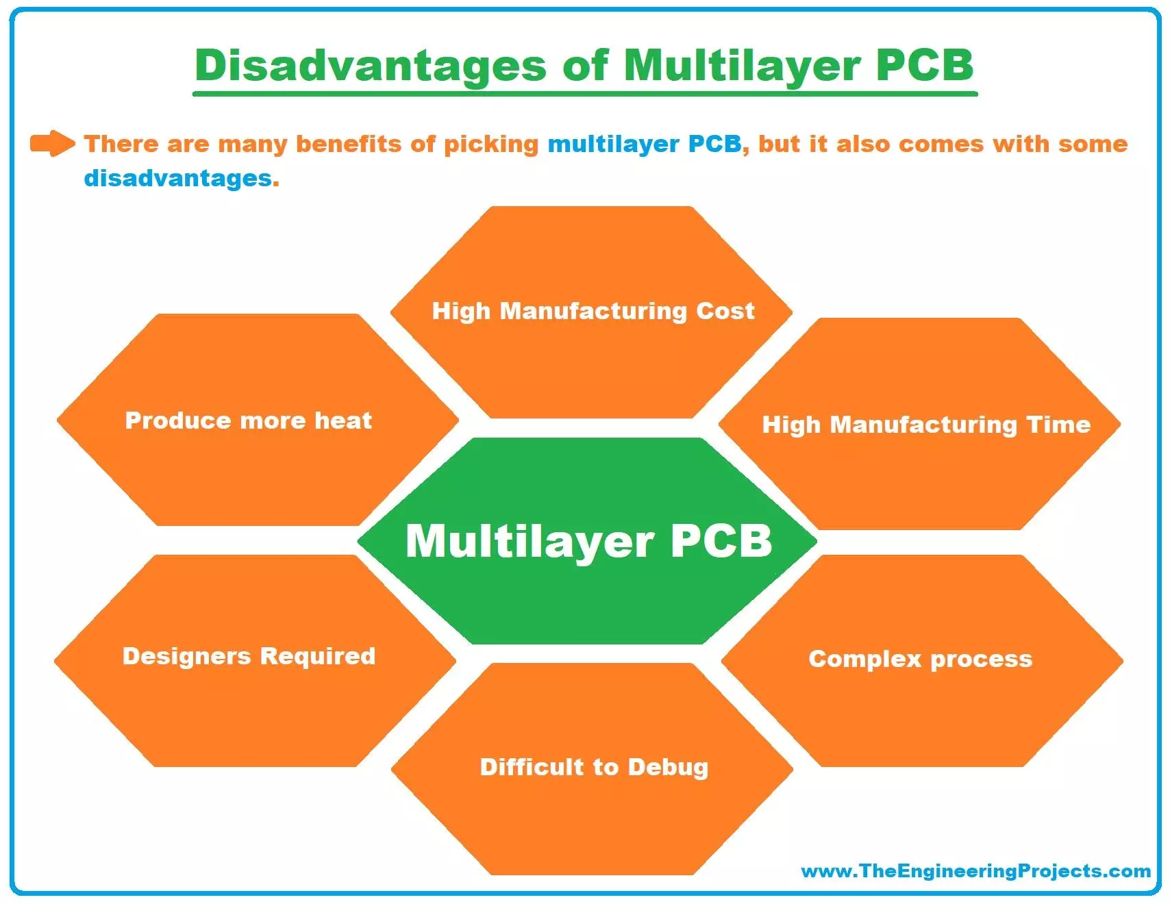
1. High Manufacturing Cost
- High manufacturing cost is the main disadvantage of Multilayer PCB.
- Online PCB companies from China provide competitive rates, but as the Multilayer PCB Manufacturing process is quite complex, thus it's a bit expensive.
2. Increased Manufacturing Time
- As compared to single/double layer PCB, multilayer PCB requires more manufacturing time as it involves a lengthy process i.e. printing, lamination, joining, etc.
- It depends on the complexity & quantity of your products but normally takes a week for a simple order.
3. Difficult to Debug/Repair
- As Multilayer PCBs are pre-assembled(from PCB Manufacturers) and involves SMD components, thus it's too difficult to debug or repair(if there's a fault) them as compared to simple PCBs.
- Companies normally design a prototype first to remove all errors/bugs and then go for professional design.
4. Professional Designers Required
- Designing a Multilayer PCB is not an easy task, as if there's a designing error present in the model, you have to redo the manufacturing process.
- So, PCB designing is normally carried out by a team of professional designers .
- Depending on the complexity of electronic design , it may involve multiple teams.
Applications of MultiLayer PCB
In the technology world, Multilayer PCB has become an essential requirement of electronic products. From binocular to radar systems, Multilayer PCB has found its way everywhere. Let's have a look at few applications of Multilayer PCB: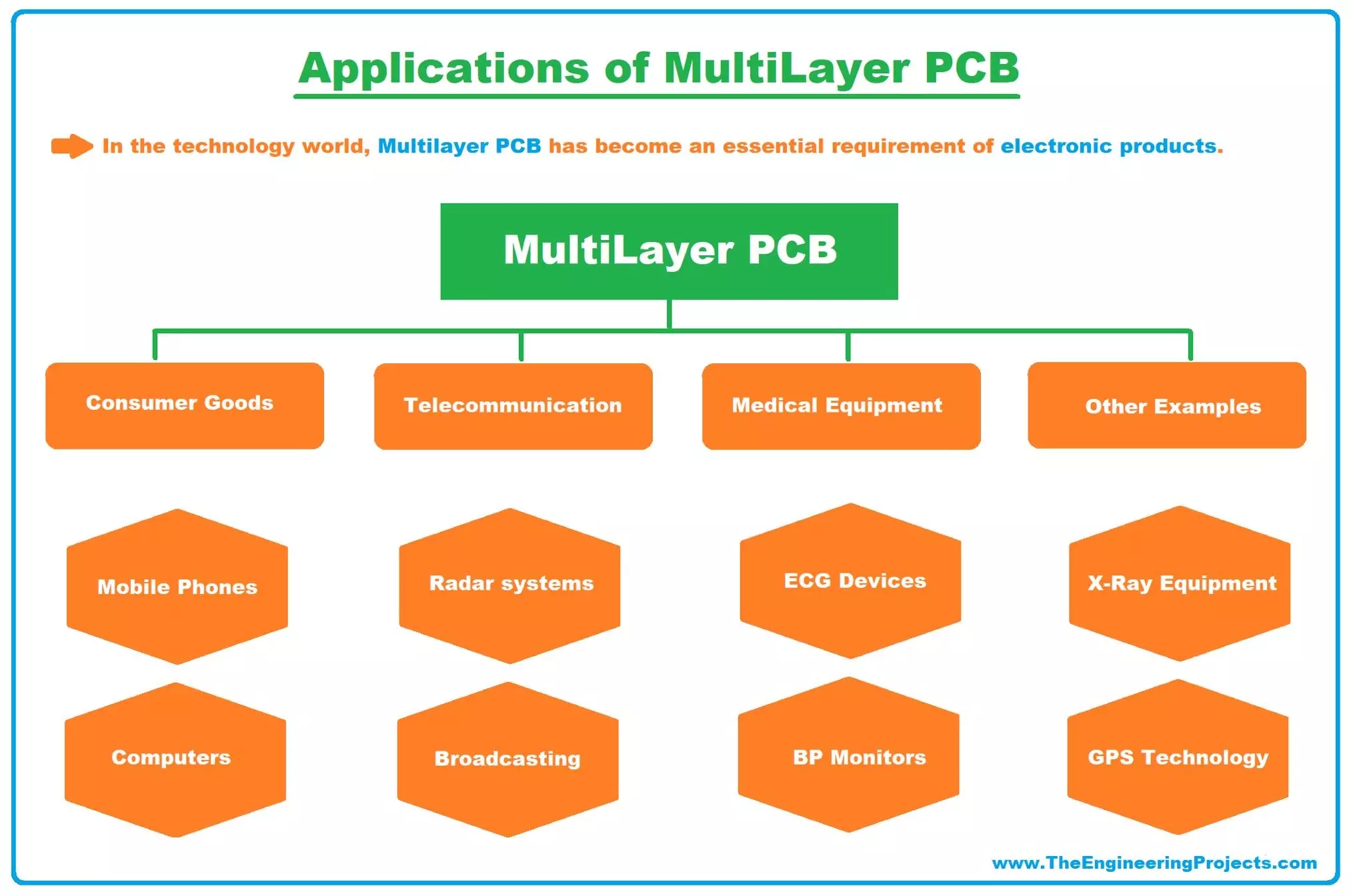
Consumer Goods
Nowadays, the human race is the slave of electronic appliances, which have become smaller, light-weight, and more functional because of Multilayer PCB. Here's a list of few consumer goods , designed using multilayer PCBs:- Home Automation systems.
- Mobile Phones.
- Computers.
- Microwaves.
- Iron.
- Shaving Machines.
Transmission/Telecommunication Systems
Data Transmission plays a vital role in everyone's life today but most of us are not aware of what's happening behind the scene. Our mobile operator companies have big transmission plants/units where thousands of multilayer PCBs are working day & night, providing us a working mobile network. Few transmission/telecommunication systems containing multilayer PCBs are:- Broadcasting systems.
- Radar systems.
- Mobile transmission systems.
- Signal transmission systems.
Medical Equipment/Devices
There was a time when big ugly machines(at government hospitals) were used for blood pressure monitoring, while today we have small hand-held electronic devices to measure blood pressure. All these smart medical devices contain Multilayer PCB in them. Few examples are:- Heart Rate Monitors
- Blood Pressure Monitors.
- ECG Devices.
- Blood Sugar Monitoring.
Few Other Examples of MultiLevel PCB
As there's a long list and we can't enlist all of them but here few other examples of Multilevel PCB :- Atomic accelerators
- Central fire alarm systems
- Weather analysis
- Space probe equipment
- X-Ray Equipment
- GPS Technology
- File servers
- Data storage
- Cat scan technology
- Fiber optic receptors
That's all for today. I hope you have found this article useful. However, if still you feel skeptical or have any questions you can ask me in the comment section below. I'd love to help you according to the best of my expertise. We always love when you keep coming back for what we have to offer that resonates with your needs and expectations. Keep your feedback and suggestions coming, they allow us to give you quality work that helps you fill with the most relevant and useful information. Stay Tuned!


