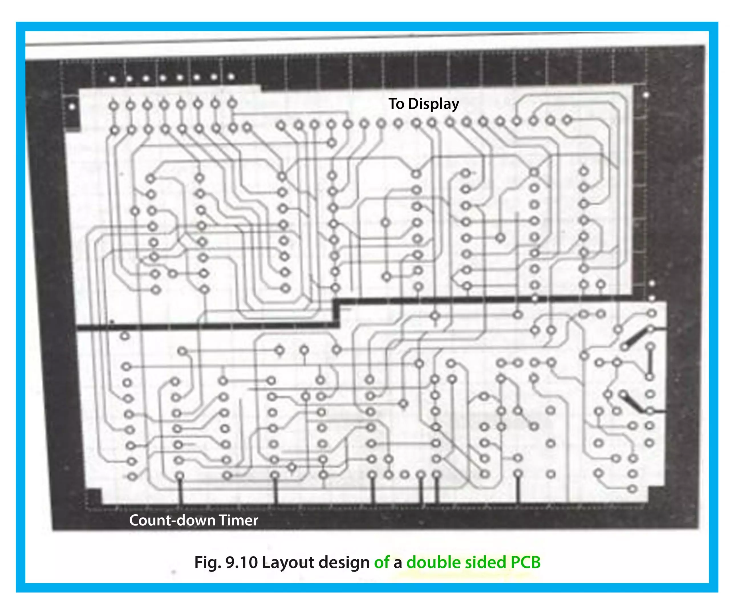
Introduction to Double Layer PCB


Before discussing the double layer PCB. we must have an idea about what’s PCB.
PCB and its classification
PCB is an abbreviation of printed circuit boards. PCB may be a sleeky chip created by compound epoxy glass fiber or laminated completely different substances. It includes a plate of insulated substantial and a sheet of copper foils coated to the substrate.
Criteria of Classification of PCB
PCBs are classified according to their number of layers and holes on them. There are three types of PCB depending on the number of their layers.
- Single-layer PCB
- Double-layer PCB
- Multilayer PCB
Now to move our attention back to our article which is double layer PCB
Introduction to double-layer PCB
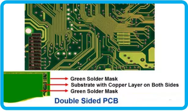
A double-sided PCB is also known as a Two-layer PCB is a kind of PCB that has a copper layer on both sides aboard. Here copper layers means the conductive layers. Simply we can say that it Comes with two conductive patterns on two sides of the base material which is called the substrate. The pattern on the sides is connected using a connection bridge which is known as VIA.
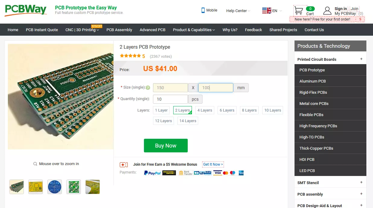
2-Layer PCB Pricing
- Let's have a look at the pricing of 2 Layer PCB, so I am going to take the example of PCBWay Fabrication House.
- If you have a look at the below figure, you can see that, if we place an order of:
- Size: 150x100mm
- Quantity: 10
- Layer: 2
- It will cost us $41 in total, and it's quite affordable.
- The price per PCB board decreases as you increase the quantity.
What is via?
Via is a hole in the vertical direction on the PCB board which is filled with metal foils due to which we connect the writing patterns.
- The area of double-sided PCB is twice that of single-layer PCB that allowing it to be used in vast applications with high-density components
Purpose of double-sided PCB
- The main purpose of this board over single layer PCB is that on this board we can connect components on one side with the other due to the presence of the hole on it. We can easily tackle with connections on this board although it is no easy task to develop a double layer PCB.
Types of double-layer PCB
There are two types of double-layer PCB.
- Without through-hole metallization (non-PTH)
- With through-hole metallization ( PTH)
PCB Manufacturing Process
Following steps are included in making a PCB:
- Initialization
- Optical lithographic
- Etching
- Stripping
- Plating of tin
- Drilling
- Testing
- Component loading
- Soldering
Initialization
- First of all, we must have a print of layout which may be obtained from Computer-aided machine, then cut the copper layer according to requirements and make sure that board is clean and free from any dust than mounting holes on it.
Optical lithographic
- In this step, we may transfer the copper tracks by exposing them to radiation sources like UV radiations
Etching
- This is used to remove the copper-clad which is unnecessary. For this purpose the board is dipped in the etching solution and remains in solution for 6 to 7 minutes at 40° C . There are many types of etching solutions like
- Ferric chloride
- Cupric chloride
- Alkaline ammonia
Stripping and tin plating
- In this step final touch is given to the copper layer on board and plating is optional which protects the copper from being oxidizing.
Drilling and testing
- In this step, components are created on board of different widths. This may be done by using manually operating drill machines by using CNC drilling machines.
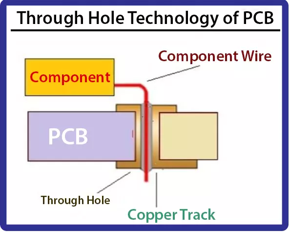
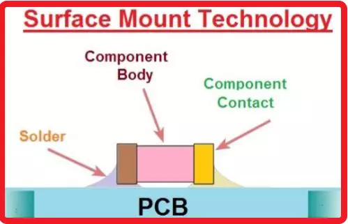
Techniques for interconnecting components onboard
Technically two methods are used for this task.- Through-hole technology
- Surface-mounted technique
Through-hole technology
- It is a technique in which we can make an electric circuit by using a wire which passed through holes and bored into PCB. In the late 1980s, every component was pointed through this technique on PCB.
Surface-mounted technology
- In this technique, there is no separate use of Wire. In its place, we can join components straight to chips which reduces space requirements.
Construction of double-layer PCB
- The construction of this board is alike to single-layer PCB, its construction is delineated here with elaborate.
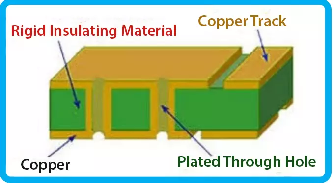
- In this circuit substrate is factory-made by the fiber or epoxy resins, the sort of base material depends on rigidity and adaptability of aboard.
- In the double layer PCB, PCB over base substances copper lamination is done to supply a semi-conductive method for parts.
- To protect From setting each side of the Board contains a solder mask over copper covering.
- There exists a silkscreen on top of the sides whose purpose is to able a person to add symbols and character on board so that a standard person will perceive the Board function.
- Double-sided PCB area units are terribly like single-sided PCB except that they need two-sided traces with high and bottom layers. These boards will mount conductive copper on either side of the card that permits the trace to cross over one another. This leads to the next density of circuit while not the Requirements of point to point fastening. These kinds of circuit boards area units are a lot of advanced than single-sided PCBs that are often harder to supply. However, the advantage of victimization double-sided PCB so much outweighs the con’s
Double-sided circuit boards are one of the foremost well-liked kinds of PCBs. They allow makers to supply a lot of advanced circuits which may have profit uses in higher technology applications.
Advantages of double-layer PCB over single layer PCB
- The most important point is that number of interconnection are approximately double that of single-sided PCBs
- They are more flexible and have easier electrical interconnections.
- Single-layer PCB has only one conducting layer over base material while double layer PCB has two conductive layers on both sides of base material known as a substrate which is made of fiberglass and is compact in its sense.
- Both double layer PCB and single layer PCB works as an electronic catalyst to deliver power to other components
- Double-sided PCB tends to increase the circuit density and reduce the overall cost.
- Although double-sided PCBs have complex circuits as compared to single-sided PCBs they are perfect and more suitable for advanced electronics because they can be used on both sides which reduces the side of the board in return reduces the overall cost.•The most important advantage of double-sided PCB is that we can repair and rework their connections.
Disadvantages of double-layer PCB
- We need very careful attention for manufacturing of layout of double-sided PCBs especially in the distribution of power across the different components.
- As they have the open structure of circuit loop there may be a chance of EMI radiations which may change the crosstalk between closely spaced tracks overboard
Application of double-layer PCB
- Due to the availability of flexibility in their structure, Double-sided PCBs are used in many applications for various purposes.
- High low temperature and solder coating are one of few important applications of Double-layer PCB.
- Double-sided PCBs are used in merchandising machines, amplifiers, automotive dashboards, and plenty of lots.
- Double-layer PCBs are used in the red lightning circuit which makes the light circuit.
- Double-layer PCBs are used in printers.
- Double-sided PCBs are used in Industrial controls for various purposes.
- Double-sided PCBs are used for instrumentation.
- Double-sided PCBs are used for testing the types of equipment.
- Double-sided PCBs are used in power supplies and hard drives.
- Double-layer PCBs are used in converters.
- Double-layer PCBs are used for control relay purposes.
- Double-layer PCBs are used in the Automotive dashboard for controlling the different functions.
- Double-sided PCBs are used in traffic systems
- Double-sided PCB has wide use in vending machines.
- Double-layer PCBs are used in inline reactors.
Conclusion
In the end, we concluded that double-layer PCBs have two layers than a single layer which has one layer. Due to advanced technology requirements, we need double-layer PCBs. Double layer PCBs are less costly but they have innovative features than single layer PCBs. This worthy feature is the demand of the modern era. Double layer PCBs have worthy applications. It also has some drawbacks which demanded that we have to develop PCBs that are effective than double-layer PCBs. You always need to opt for which kind of PCBs you would need.
That’s all for today’s article. I hope you've got enjoyed the article and built a grip on the understanding points. However, if you continue to face any skepticism concerning double-sided PCB then please be at liberty to depart your queries within the comment section. I'll give a solution to those inquiries to the simplest of my data and researching skills. Also, give North American country along with your innovative feedbacks and suggestions you improve the standard of our work and supply you content in keeping with your wants and expectations. keep tuned! thanks for reading this text.