A Detailed Guide on PCB Fabrication Process
If you don’t want to undergo this intimidating fabrication process of the board, you can get help from the online PCB manufacturers. We are quite satisfied with PCBWay services, so I am going to recommned this one.
Main Types of Printed Circuit Board
Circuit boards are categorized into three types.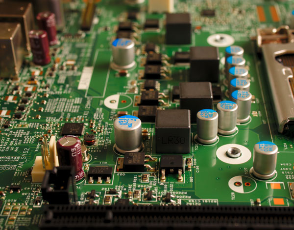
Single-sided Circuit Boards
Single-sided PCB, also called single layer PCB, is composed of woven glass epoxy material which is incorporated with copper traces on one board side and another board side is utilized to put components on the board. These copper traces electrically connect the different components on the board.Double-sided Circuit Boards
Double-sided PCB, also called two-layer PCB, is made of the same rigid woven glass epoxy material that is used in single-sided PCB, and there’s a little difference. Here both board sides are incorporated with the copper traces. And traces are kept with different thicknesses depending on the application.Multiple-sided Circuit Boards
In Multi-layer PCB copper foil is employed rather than a copper coating. This copper foil helps in the construction of different layers until you reach the required number of layers.Main Parts of PCB
Let’s elaborate on the basic parts of the PCB before documenting the fabrication process.Substrate
This is termed as the PCB skeleton – the most fundamental structure of the board. Fiberglass is utilized to construct the substrate material. Fiberglass confirms the core strength, making board strong, stern, and solid.Copper Layer
The following part is the copper layer. Depending on the PCB type, copper coating or copper foil is employed on one side or the two sides of PCB. This copper layer is used to provide an electrical connection between the board’s components. This is like the nervous system of the brain that contains neurotransmitters to communicate with the body muscles.Solder Mask
On the third number comes the solder mask. It is a defensive layer composed of a polymer that goes about as a PCB skin. It helps in securing the copper layer. It also helps protect the board from short-circuiting.Silkscreen
Silkscreen, also called legend or nomenclature, is the last part of the PCB. It is normally smeared on the board’s component side. This layer is utilized to demonstrate logos, switch settings, part number, test points, and component reference.PCB Fabrication Process
In this part, we’ll demonstrate the PCB fabrication process in detail.Step 1: The Initial Design
Everything begins with the fundamental design. A comprehensive PCB design is made on the software. There are multiple software used for the PCB design including Altium Designer, Eagle, OrCad, Pads, Proteus or KiCad When the design is made, the document is then exported. Most manufacturers support the extended Gerber file… so be sure your final document is exported in the Gerber file.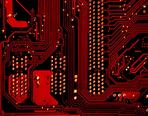
Step 2: The Print Process
The PCB is printed using the plotted printer. It produces the resultant film which is made of different layers. The black ink shows the conductive copper traces on the other hand the clear ink represents the non-conductive portions. This is used for inner layers. On the layers outside this pattern is switched for example the clear ink demonstrates the conductive copper traces and black ink shows the non-conductive regions.Step 3: The Substrate Material
Recall, the substrate is considered as the skeleton of the PCB that is made of fiberglass. This fiberglass behaves like an insulating material that is used to connect the various elements.Step 4: The layers
In the fourth step, resist is made that is composed of photosensitive film. Photo-reactive chemicals are used in this resist. When these chemicals come under the UV light, it helps in hardening the resist.Step 5: Hardening the Photoresist Layer
In this step, underlying copper pathways are revealed. Which is achieved by hardening the photoresist layer. The photoresist layer gets hardened when a combination of resist and laminate is exposed to the UV light.Step 6: Removal of Unused Copper
In this step, unwanted copper is removed. Unwanted copper is removed using the alkaline solution. While you’re at this process, be careful that it doesn’t affect the photoresist layer.Step 7: Inspection
Optical inspection and layer alignment are done in this step. Both the outer and inner layers are aligned using the holes.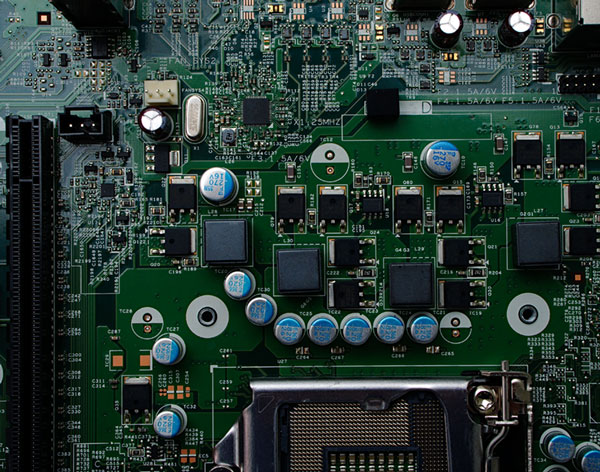
Step 8: Lamination Process
At stage 8, both outer and inner layers are pushed together for the cover. These layers are fused whenever they are examined, ensuring they are without any defect. These layers are aligned using the Prepreg made of epoxy resin. Metal clamps are used to set everything in place. The Prepreg material is covered with the substrate and copper foil. Everything is kept in place using pins and the mechanical press is employed to punch everything together. When heat and pressure are applied to the epoxy material, it melts down causing layers to fuse together. The actual PCB is then removed by removing the pins and press plates.Step 9: Drilling Process
After stage 8, the drilling process is carried out. An X-ray machine is used to locate the drill spots before applying drilling on the layers. Holes are created using a computer-guided drill. Leftover copper is then removed after the drilling process is completed.Step 10: PCB Plating
After the drilling process, a specific compound is applied to weave all layers together. This process is called PCB plating. A series of chemicals are then used to cleanse the PCB layers. The copper layer is applied between the drilled holes and on the top of the layer during this bathing process.Step 11: Outer Layer Imaging
Another layer of photoresist is employed at the PCB outer layers once the PCB plating is done. This photoresist layer is then exposed to UV light which hardens this layer. In this process, again PCB plating is applied using certain chemicals that again helps in fusing the layers together.
Step 12: The Etching Process
The tin guard is created during the last process. During the etching of this outer layer, the tin guard is utilized to secure the copper layer. After this process, unused copper is removed while the tin guard developed during the last process still protects the copper present on the outside layer.Step 13: Applying the Solder Mask
When the unused copper is removed it results in the making of proper PCB connections. In this step, we do solder masking. The final PCB panels now undergo the bathing process before we employ the solder mask. Ink proxy is used with the solder mask after the cleaning process has been finished. Then the product undergoes the UV light which results in the removal of the unused solder mask. After this step, we put PCB in the oven that develops the green colors on the PCB panels.Step 14: Final Surface Finish
In this step silver and gold materials are applied to produce the final surface finish. These materials ensure the core strength of the PCB layers and help in improving the elements bonding. After plating the PCB layers with materials like silver and gold, silk-screening is applied. In this silk screening process the necessary details like manufactures marks, company ID, warning labels are then applied to the layers of PCB.Step 15: Electrical Testing
In this step, electrical tests are applied to the PCB layers to confirm the functionality of the PCB layers. Two tests are applied… one is a circuit continuity test and the other is the isolation test.Step 16: Final Cutting Step
In this final step cutting process is carried out the removes the PCB from the original pane. A CNC machine or V-groove is used to remove PCB from the original panel. The final PCB is now ready to be used in an electrical project.
×
![]()


