


Introduction to LED PCB


In PCB boards you come across LEDs fixed in them, and due to the evolving world of technology, things are changing so first leading to the crafting of new technologies that have led to changes in the LED areas. The LED case is an area that has involved the combination of two methods of technologies in order to come up with something else that is more efficient when it comes to solving the intended purpose. This LED PCB comes with advantages of longevity and durability.
Introduction to the LED PCBs
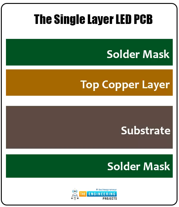
This is a type of PCB that is used for the purpose of lighting in the lighting appliances like modern LED bulbs. The material used in the process of making this board currently is the metal copper clad that has a very good heat-dissipating function. In general, we should note that the single layer LED PCB is made up of three layers namely the circuit layer, the ceramic layer and the insulation layer.
- The LEDs are laid directly in the circuit layer where they are mounted.
- The heat that comes out of the LED is quickly linked to the substrate layer for dissipation. This is done through the insulation layer then dissipated through the substrate layer.
- Copper, aluminum and iron are the most used thermal conductive layer material since they are readily available.
- The iron core is mostly used in motor high-end PCBs that have a lot of heat dissipation.
How to order LED PCB online?
There are numerous online PCB companies, where we can place the LED PCB order. We are going to take the example of PCBWay Fabrication House, a well renowned PCB Manufacturing House. They have an excellent support team, and it's recommended to first discuss your PCB design with the team, they will guide you at every step. So, follow these steps to place an order of LED PCB on PCBWay:- First of all, create an account on the PCBWay official site.
- After that click on the PCBWay Calculator, which is an excellent tool to get the quote for your PCB order.

- As you can see in the above figure, I have selected Aluminium PCBs, as LED PCBs are normally aluminum PCBs to avoid heat dissipation.
- Now click on Calculate and get the quote for your order.
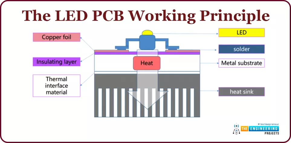
The LED PCB working principle
- The LED is mounted on the surface of the circuit layer and the heat that is generated when the PCB is under operation is quickly passed to the metal base layer via the insulating layer.
- This heat is then passed out by the metal base layer to achieve the purpose of heat dissipation of the device.
- See the attached diagram for a better understanding of the process;
LED PCD structure
Circuit layer
This is made up of the electrolytic copper foil and is etched to form the printed circuit board where the components are attached. When you do the comparison with the traditional boards, the LED board can carry a larger amount of current.
Insulating layer
This layer is the core technology behind this type of boards and plays greater roles in the conduction insulation and bonding of the layers.
Metal substrate layer
Here aluminum is the best choice compared to its availability and the cheap prices it offers. Stainless steel, silicon and the iron can be used if the thermal conductivity required is very high.
Types of the LED PCBs
The single layer LED PCB
This consist of the substrate layer together with a conductive layer. A solder mask together with a silkscreen offer protection functions to these layers.
- This type of the LED PCB does not have any circuit layer on the back side.
- Their structure is very thin and they are very weightless.
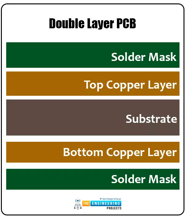
Double layer PCB
When you don a comparison with the single layer PCBs, you will realize that this has two copper layers which apparently makes them heavier as the number of conductive layers also increase to two.
- Double layered PCBs are durable since this type of circuit layer can withstand the high currents applied and it has the best heat dissipation mechanism.
Assembly methods of the LED PCB
There are two assembly methods that can be employed in the assembly if the LED PCBs. These methods are used to attach components on the board and we shall discuss it below;
Surface-mount assembly
This method involves mounting the electronic components directly into the board copper layer.
- the process is highly automated and offers flexible connections and offers spaces for high density connections.
- They play great roles in circuitry that require high connections and accuracy.
Through-hole assembly
This method involves the drilling of holes into the PCB boards where components are then mounted to the holes using the long leads that are then soldered and the whole filled with flux.
- The process involves a lot of inspections to make sure that the great accuracy and the effectiveness are achieved.
- This method off course provides a strong board with long durability.
Considerations while designing the LED PCBs
- Ideal board design; you must figure out which is the ideal board design that you should incorporate. In engineering everything starts with the design. It is the first step that comes in.
- Picking the proper orientation; when we talk about orientation, we are after how the flow of the circuit is achieved from one end to the other. The way in which the data and the electricity flow in the circuit is what we are referring to us the orientation.
- Component placement; in addition to the circuit and the obvious LED, there are many other components that form the printed circuit boards. these components include the resistors, the capacitors, etc. the components should be placed such that they avoid the solder side of the board were solders lie behind the through hole side of the board.
- Avoid placement of the components on the PCB outline; this will help you manage the board better and also ensure that the design is sturdy and very reliable.
- Vias should not be placed at the end of the STM Pads; vias allows the placement of circuits in tow or more layers if the PCB boards. these vias can go through the surface of the top layer through to the bottom layer. Avoid passing the via through the pads of the surface mounted devices since this will weaken the components.
- Definition of the net width design; due to consumption of different current in the circuits, the design paths will vary with the size of the tracks and this will also affect the net width of this design outcome.
- Cost optimization and the budget issues; this is how the overall budget of the designed PCB will go up to. Therefore, this must also be considered when coming up with the LED PCB.
Industrial applications of the LED PCBs
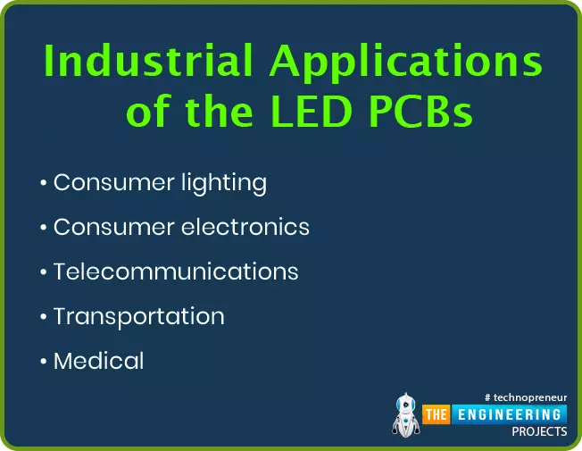
Consumer lighting
This is one of the common applications the LED PCBs where they find great use on the consumer lighting from flash lights, lamps, spotlights, lanterns to solar powered lighting applications.
Consumer electronics
LED are also becoming a common application in the electronic devices such as the computer keyboards backlights. Other devices that have employed this technology are smartphones, tablets and the televisions.
Telecommunications
Telecommunication displays and indicators use the LED PCBS because of their durability the ability to transfer heat and their longevity since telecommunication gadgets generate a lot of heat.
Transportations
LEDs have a lot of use in the traffic and the transportation industry ranging from the stop lights and the automotive themselves. In the car this PCs are found in the headlights, fog lights, brake lights, reverse lights and the indicators. Highways tunnel lighting also use this technology. The modern streetlighting system is done using the LED PCBs.
Medical
Medical lighting and the medical equipment lighting that are used for medical examination and surgery often use this type LED PCBs.
Benefits of this LED PCBs
- Reduced consumption of power
- More efficiency compared to the traditional boards.
- They are smaller in size
- This type of board is mercury free
- It is radiofrequency free
- It is much environment friendly
- Cheap and this implies reduced cost.
- It has a longer life compared to others.


