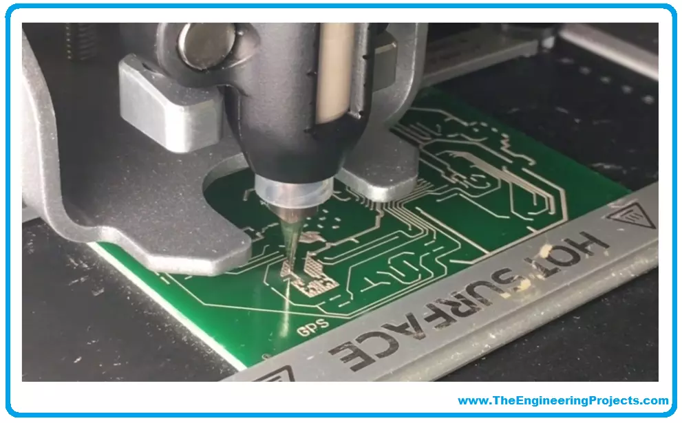
Quick-Turn PCB Prototyping Service


Hi friends, I hope you are enjoying yourself a lot and having a great deal of fun. Our mission is to help you by providing quality content that meets your expectations so now today we will discuss all quick turn PCB prototyping services. We will discuss what is quick-turn PCB? What is a PCB prototype? What is a quick-turn PCB prototyping service? Quick turn PCB general Capabilities provided by companies. Benefits, applications and importance of quick turn prototyping service. Online Quick-turn PCB service providers and time measurements. So, let's get started:
Overview
- First of all, before starting the discussion we have to know about the meanings of the words used in our topic heading.
- We have to make grip on the meanings of quick turn, PCB, prototype, and service. After understanding the heading of the topic we will be able to understand core concepts.
- Quick turn: quick turn means something or someone that does things with great speed. Day traders use the quick turn technique to make a great deal of profit.
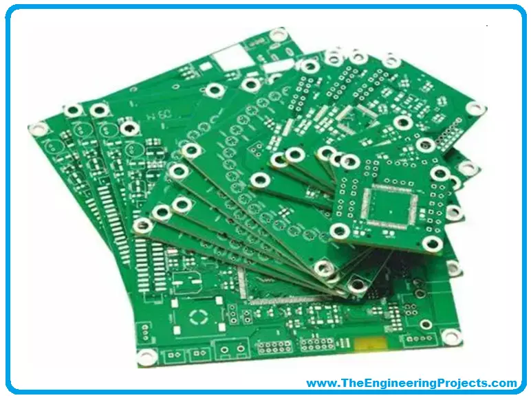
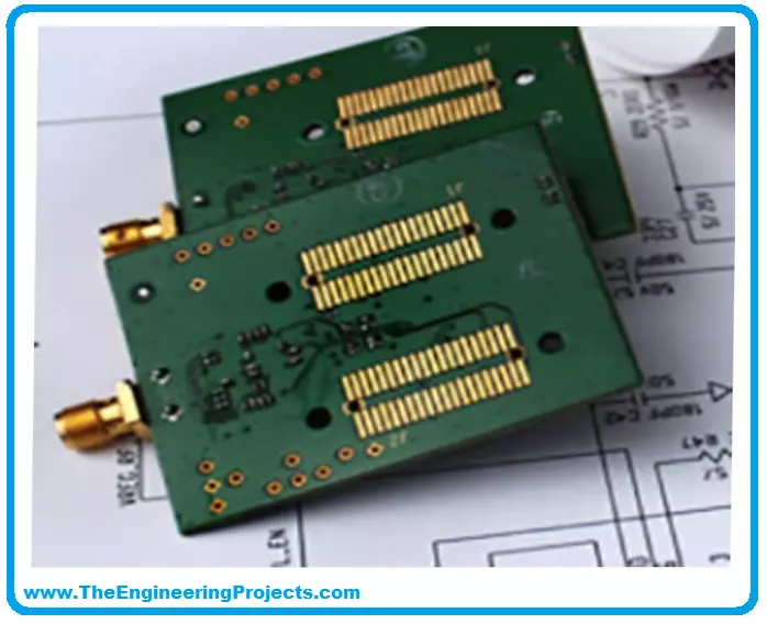
- PCB: PCB stands for the printed circuit board. It is a combination of conductive and insulating layers to perform specific functions that meet the demands of customers.
- The prototype is defined as an original model on which something is patterned. It is an early sample product built to test a process or concept.
- Now prototyping is a fundamental process for designing a new product on which electrical components will be patterned.
- Service: service is a system that is used to provide utilities like providing PCBs to the provided/desired location.
What is a quick turn PCB?
- Now after understanding the meaning of each term used in the heading we have to understand what is quick turn PCB? What is PCB prototyping and then we will discuss what is quick turn PCB prototyping service?
- A quick turn PCB means that a customer has their PCB faster than ever before.
- A quick turn ensures that a customer doesn’t have to wait for their product so it reduces delays.
- A quick turn also ensures that the manufacturing time for the PCB is reduced.
What is PCB prototyping?
- A PCB prototyping is to help designers to determine if there are any faults in the original PCB.
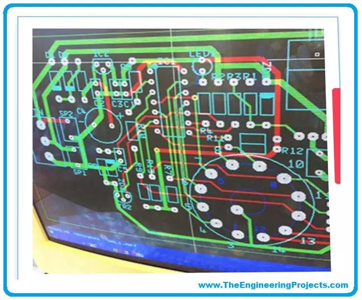
- It helps to improve performance and enhance efficiency.
- As prototypes are crucial so it is very difficult to make changes in the PCB which is manufactured.
- Quick turn PCB prototyping service means that providing PCB prototypes to the customers at a very fast speed, without delay.
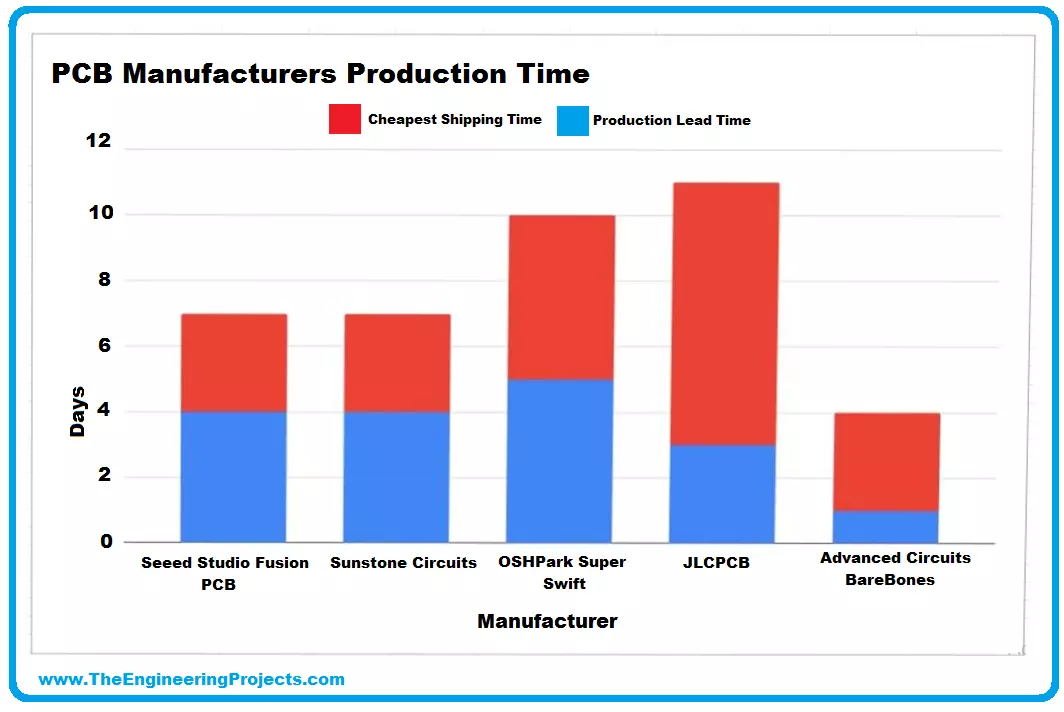
Online Quick turn PCB prototyping service providers:
There are some online quick turn PCB prototyping service providers available. The one I am going to recommend is JLCPCB Fabrication House. JLCPCB provides this service of Quick-Turn PCB Prototyping for researchers so that they could test their projects in no time. Here are a few of the key points of this service provided by JLCPCB:- They provide 1-50 layer PCBs with PCB Order Quality < 1m2 within 24 hours, while normally it takes 2-3 days for accomplishing such tasks.
- For PCBs with order quality between 1m2-5m2, JLCPCB takes around 3-4 days, while the normal time range is 5-7 days.
Few other Quick-Turn PCB suppliers are:
- pcb4u.com
- pcbway
- aipcba
- pcbunlimited
- pcbgogo
- Homebrew fabrication
- Breadboard killer
- Foundation technology
- Linksprite
- Kingfield electronics- CEM services
- Apex
- Cadsoft Eagle
- Exception group
- Bittele electronics
- Technotronic
- 4pcbassembly
- Sinomicro PCB
- Asian circuits
- Standard printed circuit board limited
- PCB train
- Euro circuit.....etc
PCB Capabilities - Quick-turn PCB
- Providing PCB prototypes within 24-72 hours is the quick turn PCB prototyping service.
- Companies do not have to look eye only at providing PCB at a fast rate but they don’t have to compromise on the quality of the product.
| Items | General Manufacturing Capabilities | Companies general Remarks |
| How many layers | 1-10 layers | For orders above 10 layers, contact to company. |
| Material | Aluminium or RF-4 | For Flex, Rigid-flex, Metal-based (Aluminium etc.,), HDI, Halogen-free, High Tg, etc. |
| Maximum dimensions of PCB | 500*1100mm (min 5*6mm) | For any size Greater than these Standard dimensions customers have to contact to the company |
| Tolerance in board size | ±0.2mm/±0.5mm | ±0.2mm for CNC routing, and ±0.5mm for V-scoring. |
| Thickness of the board | 0.2-2.4mm | 0.2,0.4, 0.6, 0.8, 1.0, 1.2, 1.6, 2.0, 2.4mm. For other thicknesses, customers have to contact to company. |
| Tolerance in the thickness of board | ±10% | Normally “+ Tolerance” will occur due to PCB processing steps such as solder mask, electroless copper and other types of finish on the surface. |
| Board Thickness Tolerance(t<1.0mm) | ±0.1mm | |
| Minimum manufactural Trace | 0.1mm | Min manufactural trace is (0.1mm), To save cost design trace should be above 6mil(0.15mm) |
| Min Spacing | Min manufactural spacing is 0.1 mm. To save cost it should be 6mil(0.15mm) | |
| Thickness of outer copper layer | 1oz/2oz/3oz(35µm/70µm/105µm) | Also known as copper weight. 35µm=1oz, 70µm=2oz, 105µm=3oz. For copper weight greater than 3oz customers have to contact the company. |
| Thickness of inner copper layer | 1oz/1.5oz(35µm/50µm) | Inner copper weight as per customer’s request for 4 and 6 layers is 1-1.5 oz. |
| Drill Sizes | 0.2-6.3mm | Min hole size is 0.2mm, max drill size is 6.3mm. Any holes greater than 6.3mm or smaller than 0.3mm customer will have to pay extra charges. |
| Annular Ring’s minimum width | 0.15mm(6mil) | Min width for Annular Ring is 0.15mm(6mil), for pads with vias in the middle |
| Diameter of finished hole | 0.2mm-6.2mm | The final hole diameter will be smaller than the size of the drill because of copper plating in the holes. |
| Tolerance of finished hole size | ±0.08mm | For example, if the drill size is 0.8mm, the finished hole diameter ranges from 0.72mm to 0.88mm will be considered acceptable. |
| Solder Mask | LPI | Liquid Photo-Image able is the most adopted. Thermosetting Ink is used in the inexpensive PCBs |
| Width of minimum character | 0.15mm | Characters of less than 0.15mm wide will not be Identify easily. |
| Height of minimum character | 0.8mm | Characters of less than 0.8mm high will be too small to be identified. |
| Width to Height Ratio of character | 1:5 | In PCB silkscreen legends processing, 1:5 is the most suitable ratio for character width to height. |
| minimum diameter of PHH( plated half holes) | 0.6mm | Design Half-Holes greater than 0.6mm for better connections. |
| Surface Finishing | HASL with lead HASL lead free Immersion gold | These are the tree most popular types of surface finish. |
| Solder Mask | Black, yellow, white, blue, green, red | No extra charge (Green, Red, Yellow, Blue) |
| Silkscreen | White, Black and None | No extra charge. |
| Panelization | Tab-routing with Perforation (Stamp Holes)V- scoring Tab-routing | For break-routing min clearance between boards should be 1.6mm and for V- scoring it should be zero. |
| Others | UL certificate, Fly Probe and A.O.I. testing, ISO 9001:2008 | No extra charge. |
Quick turn PCB service types:
PCB manufacturing service providers provide PCB quick turn services as
- 1-day quick turn PCB prototype
- 2 days quick turn PCB prototype
- 3 days quick turn PCB prototype
- 5 days quick turn PCB prototype
- 10 days PCB standard PCB prototype
- > 10 days PCB prototype.
Benefits of quick turn PCB prototyping service:
- Why do designers rely on prototypes instead of making a standard product? The answer to this question is that the prototype allows designers to test the functionality of the product in the design process at several stages and allow them to make adjustments according to their needs.
- Prototyping creates several advantages for customers and manufacturers as
1. Reduced timeline:
PCB prototypes help designers to complete their final product in these ways by saving their time.
- PCB prototypes complete the testing process at a fast rate. Without prototypes, flaws will waste a lot of time, lost revenue, and make a customer unhappy.
- PCB prototypes also save time by providing visual assistance to clients during the production process.
- At several stages, Prototypes help in testing before a full production run and save not only time but also minimized rework.
2. Reduced costs:
Prototypes help in reducing cost by avoiding the following issues:
- Catching design flaws
- Pinpointing cost-saving adjustments.
- Determining product adjustments.
3. Test components individually:
Designers use PCB prototypes for testing purposes. Most beneficial testing is achieved by testing simple PCBs. This type of testing is used to achieve the purposes listed below
- Testing design theories
- Breaking down complex designs.
4. Accurate reliable prototype:
Accurately designed reliable prototypes help throughout the designing and manufacturing process. Quality PCB prototypes allow designers to test the following aspects:
- PCB design
- Functional testing
- Conditional testing
- Final product design
5. Manufacturing review and assistance:
Using third party PCB prototyping services companies gain benefits but several things can go wrong in the design process that results in mistakes listed below:
- Excessive input
- Design blind spots
- Design rule check
Applications of quick turn PCB prototype:
Quick turn PCB has several applications in different industries. The applications in different scenarios are listed below:
- Electronic designers who require high-quality boards use quick-turn PCB prototypes.
Importance of quick turn PCB prototyping service:
- The role of PCBs in the best performance of electronic devices can not be denied.
- Electronic devises based companies heavily depend upon PCB prototyping firms and their efficiency of fabrication.
- However, to meet challenging deadlines, pressing schedules, and excellent quality PCB manufacturing, quick turn PCB prototyping service plays a crucial role.
- Let’s know-how companies benefit from their quick services and attain their business goals.
- By providing quick turn services, companies increase their number of customers.
- For the projects that need to be completed in a very short time, companies charge extra amounts. To attain the goals of extra profit, and everything related to PCB manufacturing should be perfect.
- By providing reference prototyping services, companies built a trust relationship with their customers.
- Listed above are the benefits/ importance for companies providing quick turn PCB prototyping service. Quick turn PCB prototyping service is not only beneficial for companies but also for clients. Here is the importance of quick turn PCB service for customers.
- By obtaining their prototype according to their demands, customers can complete their projects on time.
- Customers do not have to waste their time in transportation and searching for PCB, they just have to order PCB and mention their requirements. Their desired PCB will be at their door.
- There are also some cost benefits to customers in this service.
Quick turn PCB prototyping service time measurement:
- When an order is placed in the morning like at 9:00 am then at next business day noon, 1 day is completed and from noon after 24 hours, 2nd day is completed from your order.
- If an order is placed at 12:00 am then after 24 hours, 1 day will be completed. And next days will be counted similarly.
- For orders placed after 4:00 pm lost much of their time so placing late time orders is not suitable.
Conclusion:
When we think about PCB prototyping, it seems an additional step that will enhance the PCB cost and we consider it one that never is overlooked. But the reality is that it is best to weed out errors, flaws, and faults before proceeding to the final product. Prototyping helps in reducing cost, provides us with quicker turnaround time, and provides you with more efficient design. Now designers always prefer prototypes before developing new innovative ideas as well. They know about the value of time, cost and quality so suggest to students, engineers, and innovators to use prototypes. In the end, we can say that the value of PCB prototypes can not be neglected, they are as fruitful and helpful as standard PCBs.
That’s all for today’s article. I hope you have enjoyed the article and make grip on the understanding points. However, if you still face any skepticism regarding single-layer PCB then please feel free to leave your questions in the comment section. I will provide an answer to these questions to the best of my knowledge and researching skills. Also, provide us with your innovative feedbacks and suggestions you improve the quality of our work and provide you content according to your needs and expectations. Stay tuned! Thank you for reading this article.