


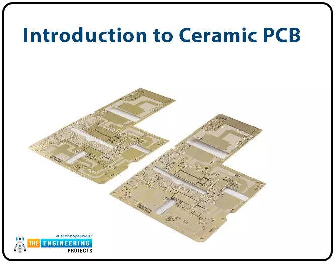
Introduction to Ceramic Printed Circuit Board


Hello friends and welcome to this article. Today we are going to have a look at the introduction to the ceramic printed circuit boards. we have previously introduced what a printed circuit board is and we noticed that it is a very important part that makes electronic circuits complete and well organized. Having that in mind, we had also discussed several materials that build up these PCBs and today our focus is on the ceramic types of PCBs.
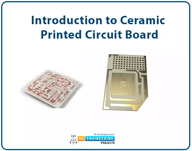
Introduction to Ceramic Printed Circuit Board
- This printed circuit board is referred to as ceramic PCB because of the substrate used in the construction of this board is made up of ceramic and it finds applications in special areas.
- The process of making this board is that copper is pasted on the surface that is made up of alumina ceramic which is the substrate material at a very high amount of temperature.
- Its substrate material offers a very high value of conductivity features, very great insulation factors and provides easy soldering surfaces.
- The most preferred manufacturing process is the laser rapid metalization technique which is a very important process.
- The structure of ceramic borders is very simple when compared to other types of these boards and it offers high-level operations than what is offered by the other type of boards.
- The size of the conductive layer used in this type of board is between one micrometer and 1-millimeter thickness.
How to order Ceramic PCB
There are many online PCB companies, where we can place our PCB orders and the best of them all is JLCPCB. JLCPCB is a China-based PCB Fabrication house and offers the cheapest PCB rates. It's quite simple to place your PCB order on the JLCPCB official site. Here are the steps:
- First of all, create an account on the JLCPCB site.
- They have an online PCB calculator, where you can calculate the final price of your order by adding all your requirements.
- Next, you need to upload the Gerber file of your PCB design.
- Finally, made the payments through an online secure payment gateway, they have multiple options i.e. Visa, MasterCard, PayPal.
- That's it, once your order got ready, you will get it through DHL express delivery service.
Structure of the ceramic PCB
In this discussion, we shall have a look at a single-layer ceramic PCB. It consists of; the ceramic substrate layer, the copper layer and the solder mask layer. Let us have a look at the image below which is a double-sided layer ceramic PCB constructed through the normal method of lamination.
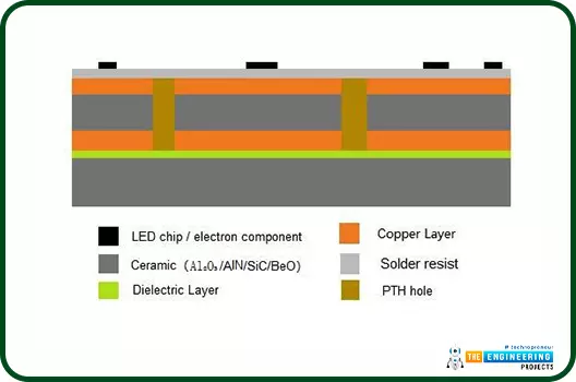
Ceramic substrate
- Compared to the FR-4, ceramic has good thermal conductivity and thermal insulation features and there in these boards, ceramic plays two very important roles one is about thermal dissipation and the other is about providing insulation between the board’s circuit layers.
- When double or multilayer ceramic PCB is required, vias are necessary for providing connection between the layers. To achieve this, vias are drilled through the ceramic substrate by the use of laser technology.
- The drilled vias are then filled with the copper core through plating.
Copper layer
- This is in form of a thin copper foil that is bonded to the substrate by the method of magnetic sputtering.
- After bonding the copper foil on the ceramic substrate, the circuit is etched on the copper by the use of the photoresist coating of the yellow light way.
Dielectric layer
- Made up of various materials such as epoxy resins, phenolic, etc.
- It is used to bond the structures of two adjacent ceramic substrate layers.
- This substrate has poor thermal conductivity properties compared to the ceramic material hence it ends up affecting the overall thermal conductivity of this board.
- it is important to note that ceramic boards can only be used in applications that have lower heat dissipation.
Solder mask
- this has the importance of protecting the exposed copper wires from solder, metals and damages from the environmental conditions.
- The solder mask is applied on the top layer of every PCB after completion of lamination. It might be white, green, beige, red, etc in color.
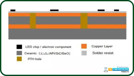
Single-sided layer ceramic PCB is shown below;
Types of Ceramic PCB
Ceramic PCBs are classified according to ceramic substrate material used and also according to the manufacturing method that was used. Let us have a deeper look into these classifications below;
Classification according to the type of ceramic substrate used
Alumina PCBs
They are the most used types of ceramic PCBs and aluminum oxide is the most readily available substrate.
Aluminum nitride PCBs
They are also commonly used PCBs but they are a bit expensive when a comparison is done with the alumina PCBs.
They gave high thermal conductivity and smartly higher frequency performance again when compared to the Alumina ones.
Silicon nitride PCBs
More costly when compared with the aluminum nitride PCBs. They have higher mechanical strength and toughness hence finding greater use in the power modules such as IGBT and military modules.
Silicon carbide PCBs
This is diamond and has high thermal conductivity and electrical conductivity. They find applications in the areas of laser technology.
Boron oxide PCBs
Has dozen times boron activities than the alumina ceramics but this type of ceramic is very poisonous. They find use in high power and frequency applications
Classification according to manufacturing.
High temperature co-fired ceramic – HTCC
This is the earliest method known for PCB manufacturing. The method is suitable for high power and not for high speed or high-frequency PCB manufacturing.
Direct bonding copper method – DBC
This one requires lower temperature compared to the HTCC. They have no PTH vias and they are mainly preserved for power electronic module packaging.
Thick film ceramic PCBs
This has a requirement that the circuit line space should be at 60 micrometers. They find their use in applications that require lower power utilization.
Low temperature co-fired ceramics PCBs – LTCC
They are usually multilayer and normally three-dimensional. They are best suited for communication devices with high frequency.
Thin-film ceramic PCBs.
Has very high precision circuits but the copper layer has a limited thickness. These types of PCBs find their use in high precision devices and also in very small devices development.
Direct platting copper PCBs
They are developed from thin-film technology and can be in 3D and has very high circuit precision. They find their use in high-frequency and high-power circuits.
Characteristics of the ceramic PCBs.
Ceramic boards have very distinct characteristics that always give them an advantage over the other type of boards. below is the list of these special characteristics;
- They are excellent heat conductors.
- Offers excellent CTA component compliance.
- With ceramic PCBs expect a high level of mechanical compatibility.
- They are not easily corroded by chemicals.
- It is very simple to do a high-density outline in these types of PCB boards.
Benefits/advantages of the ceramic PCBs
The ceramic PCB boards are given high priority due to a number of material features and characteristics that they offer which proves to be beneficial in the process of PCB manufacturing. The character of heat dissipation gives this board an advantage over the traditional types of PCB boards. components of the board are placed on the boards directly without the involvement of the isolation layer and this makes the flow of heat throughout the board better compared to the other types of boards. The following are some of the benefits that make this board the most preferred;
High thermal expansion
They are the most popular in the field of electronics due to their features that are unique. One of these features is that it provides a very high thermal coefficient expansion. These boards will still offer very high thermal conductivity even when operated at high temperatures.
Adaptability
These types of boards use a metal core. The metal core is used when the board is undergoing the engineering process. The board can be changed to a rigid carrier which will offer a stiff mechanical strength. This stiffness is very crucial as it allows the board to be used in both fluids and solids.
Durability
The ceramic material offers a lasting-results to the PCBs being manufactured. The toughness of the material used in the making of the board will protect it against routine wear and tear. In addition, these boards offer high thermal resistance which will slow down the decomposition of these types of boards and therefore increase their durability.
Stability
They offer very high stability which is a result of a stable dielectric property that originates from the dielectric materials. Due to the toughness of the ceramic materials, it has a natural resistance to many chemicals.
Versatility
It has a very high melting point hence it can be used in many applications for both low and high temperatures. The best thing about these ceramic boards is that they will offer good thermal conductivity while distributing heat evenly throughout the board and different positions of the devices.
Ceramic boards disadvantage
- It is very hard to find ceramic PCB boards because they are hardly available.
- When compared to the standard boards, the ceramic boards are very expensive.
- These types of boards are highly fragile and therefore they require handling with great care.
Ceramic PCBs applications
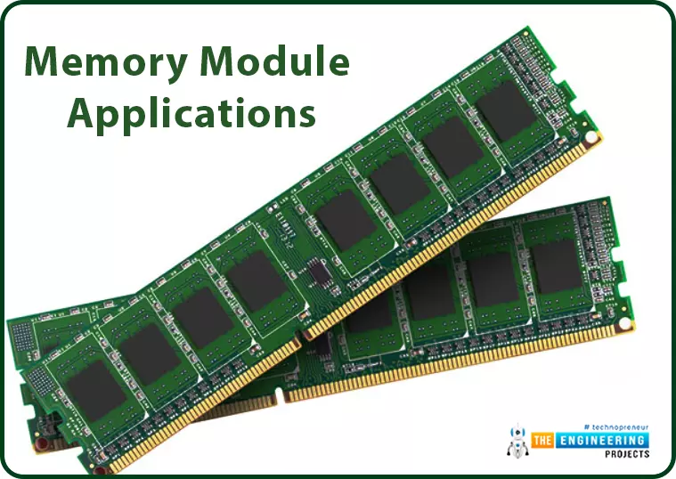
Memory module applications
It was done in Japan when a company crested an SRAM memory module by the use of the multilayer ceramic PCB. The ceramic PCB is appreciated for both high-density PCB and low-density PCB. Another example is about the USA company that had developed the telecommunication, aerospace and missile products using this type of board.
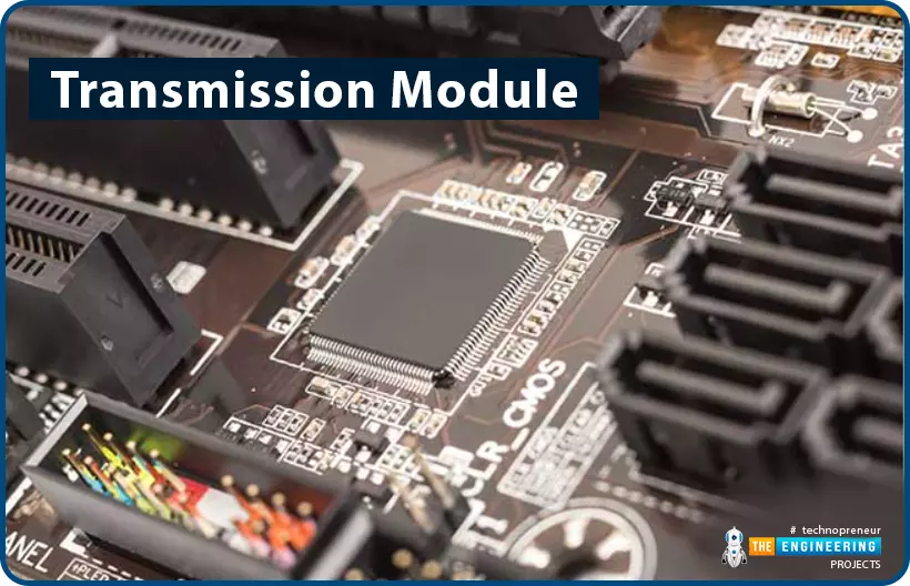
Transmission module
This is being done by an American company that is determined is building a transmission module for radar communication using the ceramic PCB boards.
Digital PCBs
Japanese have used low-temperature PCBs in the manufacture of digital PCBs. This is used because it reduces the weight of the circuit greatly. It also reduces the volume of the circuit.
Interconnect boards;
The ceramic boards are mostly used in printed circuit boards because they support the miniaturization of the devices. It has a very high probability in the application of the boards in multilayer interconnects.
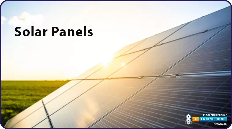
Solar panels
HTCCs and LTCCs are both applied in the process of making photovoltaic panels. In this device, we shall use multilayer ceramic PCBs to make them tough and durable.
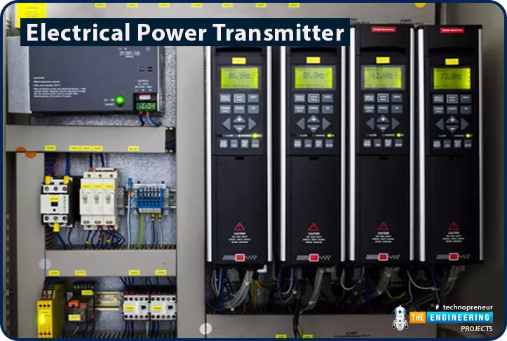
Electrical power transmitter
There has been an increase in the use of wireless power transmission systems and this implies that most power transmission system has to use ceramic boards to achieve that ability.
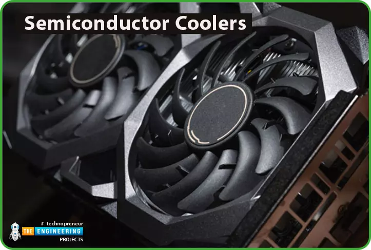
Semiconductor coolers
With the introduction of very small pocket gadgets, many electronic circuits are getting miniatured. To achieve miniaturization, it starts with the use of semiconductors that have a highly reduced size. The normal boards cannot give the support needed in order to make sure that the miniaturization process is fully achieved. In order to make this possible, ceramic semiconductors have been introduced and this is accompanied by the use of ceramic PCBs.
How to choose the right ceramic PCB manufacturer
When you are choosing the person or the manufacturer who can produce your board, you have to consider the manufacturer who has the superior tooling that is required to make the process successful. The manufacturer should be able to control the oxidation process so that the board can have superior thermal conductivity and higher temperature resistance.
Ensure that the manufacturer uses the automated process to do the manufacturing and this will make sure that your board is in perfect condition and of very high quality and the process will be less time-consuming.


