


What is PCB prototyping?


In the realm of electronics, the printed circuit board (PCB) serves as the foundation for countless technological advancements. PCBs connect and support various electronic components. They ensure seamless functionality and optimal performance. PCB prototyping plays a critical role in the development and testing of new designs before mass production. In this article, we will delve into the world of PCB prototyping. We will explore what it entails. We will also provide valuable insights on how to design and manufacture PCB prototypes effectively.
PCBWay is your one-stop solution for professional PCB prototyping services. With their cutting-edge technology and vast experience, they provide you with high-quality PCBs that meet your exact specifications. Whether you're a hobbyist or an entrepreneur, their dedicated team is committed to delivering excellence in every aspect of their PCB prototyping service.
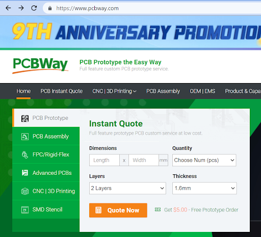
They have a very user-friendly website. There you can place your order without any hassle. Below is what the website looks like:
PCBway provides a data-based, quality PCB prototyping service. Their service is available in more than 170 countries. They have a 98.3% on-time delivery rate. They process more than 2100 orders daily.
Here you can see some of their high-profile customers:
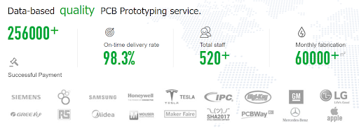
Table of Contents:
1. What is a PCB Prototype?
2. Importance of PCB Prototyping
3. Understanding the Design Process
a. Schematic Capture
b. PCB Layout Design
4. Selecting the Right Tools and Software
5. Design Guidelines for PCB Prototypes
a. Component Placement and Routing
b. Power and Ground Planes
c. Signal Integrity and High-Speed Design Considerations
6. Manufacturing PCB Prototypes
a. Fabrication Process
b. Assembly Process
c. Testing and Validation
i) DFM checks
ii) Design Rule Check (DRC)
7. Common Challenges and Troubleshooting
8. Best Practices for Successful PCB Prototyping
a. Collaboration and Communication
b. Iterative Design Approach
c. Documentation and Version Control
9. Conclusion
1. What is a PCB Prototype?
A PCB prototype is a functional sample of a printed circuit board that serves as a proof-of-concept for a specific design. It allows engineers and designers to validate their circuit design, test its functionality, and identify potential improvements or issues before proceeding with mass production. PCB prototypes typically undergo rigorous testing and analysis to ensure their reliability, performance, and manufacturability. Prototyping is an essential step in the product development cycle as it helps to refine the design, reduce costs, and minimize risks associated with full-scale production.
2. Importance of PCB Prototyping
PCB prototyping offers numerous benefits and advantages throughout the product development cycle. It enables designers to visualize their circuit design, validate its functionality, and identify and rectify any design flaws or issues. By identifying and addressing these problems early on, costly mistakes can be avoided during mass production. Moreover, PCB prototyping allows for performance optimization, improved product quality, and reduced time to market.
Prototyping also provides an opportunity to evaluate different design alternatives and assess their feasibility and effectiveness. It helps designers gain a deeper understanding of the interaction between components, identify potential bottlenecks, and optimize the layout for better signal integrity, thermal management, and manufacturability.
3. Understanding the Design Process
The design process is a crucial aspect of PCB prototyping, encompassing schematic capture and PCB layout design.
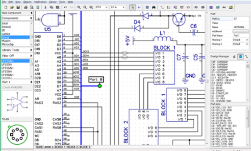
a. Schematic Capture:
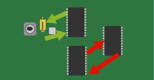
Schematic capture involves creating a graphical representation of the circuit design using specialized software tools. It involves selecting and connecting various electronic components to form a functional circuit diagram, capturing the electrical connections and relationships between components. During this stage, designers must consider factors such as the desired functionality, component availability, and compatibility.
The following image is an example of a schematic capture.
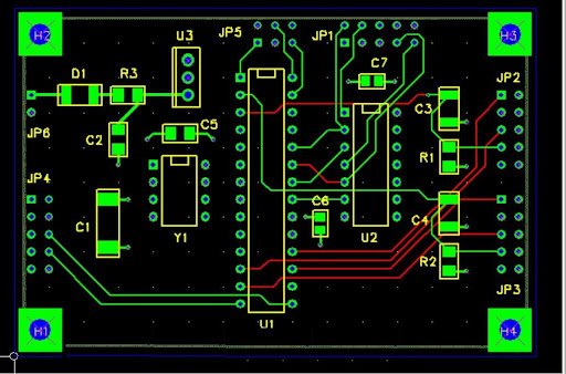
b. PCB Layout Design:
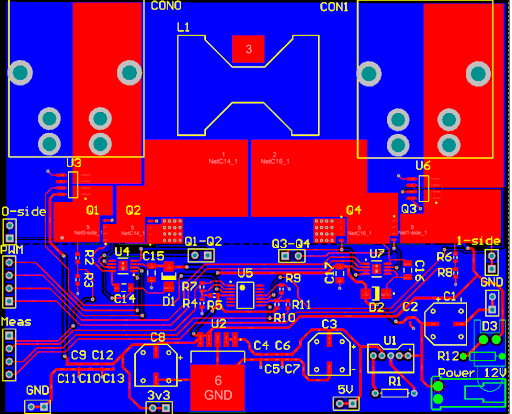
Once the schematic is finalized, the next step is to create the PCB layout design. This involves translating the circuit diagram into a physical representation of the PCB, positioning components, and routing traces to establish electrical connections. PCB layout design requires careful consideration of component placement. Designers should consider signal integrity, power distribution, and manufacturability too. Designers need to optimize the layout to minimize noise, ensure proper thermal dissipation, and facilitate ease of assembly.
Following is an example of a PCB layout:
4. Selecting the Right Tools and Software
To design PCB prototypes effectively, it is essential to choose the right tools and software. Numerous software packages are available that facilitate schematic capture, PCB layout design, and simulation. These tools offer features such as component libraries, design rule checks, and simulation capabilities, enabling designers to create accurate and optimized PCB prototypes.
When selecting tools, it is important to consider factors such as the complexity of the design, ease of use, availability of support, and compatibility with manufacturing processes. Popular software tools for PCB design include Altium Designer, Eagle, KiCad, and OrCAD, among others. Additionally, designers should also consider the availability of design resources, community support, and compatibility with the chosen PCB manufacturing service.
5. Design Guidelines for PCB Prototypes
To ensure the success of a PCB prototype, adherence to certain design guidelines is crucial. Consider the following aspects during the design process:
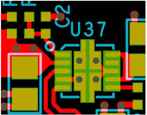
a. Component Placement and Routing:
Efficient component placement and routing contribute to optimal signal flow, reduced noise interference, and ease of assembly. Consider factors such as signal paths, thermal management, and component accessibility while placing and routing components on the PCB. Group components logically based on their functions and connections, and minimize the length and complexity of traces to avoid signal degradation and interference.
The following image shows a good arrangement of components.
b. Power and Ground Planes:
Proper allocation of power and ground planes helps ensure a stable power supply. It reduces noise and improves signal integrity. Implementing a multilayer PCB design with dedicated power and ground planes is often beneficial for high-speed and complex designs. Ensure that power and ground traces are sufficiently wide to minimize resistance and voltage drops, and employ vias to establish connections between different layers.
The image below shows the power and ground planes.
c. Signal Integrity and High-Speed Design Considerations:
For designs involving high-speed signals, careful attention must be paid to signal integrity. Consider factors such as impedance control, termination techniques, and signal routing to minimize reflections, crosstalk, and other signal integrity issues. Use controlled impedance traces for high-frequency signals, and employ techniques such as differential signaling and shielding to minimize electromagnetic interference (EMI).
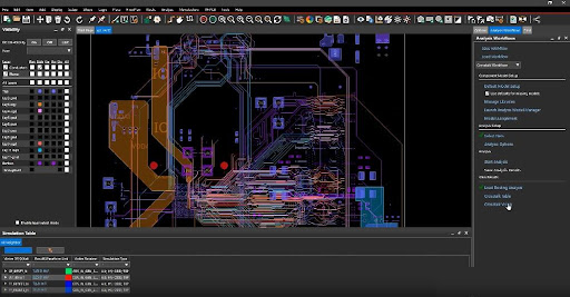
The following picture shows Crosstalk Checking in PCB Layout for Signal Integrity Validation.
6. Manufacturing PCB Prototypes
Once the PCB design is complete, the next step is manufacturing the prototypes. The manufacturing process typically involves two main stages: fabrication and assembly.
a. Fabrication Process:
The fabrication process involves translating the PCB design into physical reality. It includes steps such as creating the PCB stack-up, applying the copper layers, etching, drilling, and applying surface finishes. Advanced fabrication techniques, such as advanced routing and via technologies, are employed to meet the design requirements. During the fabrication process, designers must consider factors such as the choice of substrate material, layer stack-up, copper weight, and surface finish to ensure the desired performance and reliability of the PCB prototype.
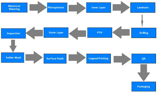
The following image shows the sequence of PCB fabrication:
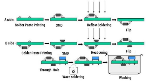
b. Assembly Process:
During the assembly process, electronic components are mounted onto the fabricated PCB. This can be done through manual or automated processes, depending on the complexity and scale of the design. Once the components are placed, they are soldered onto the PCB, and any necessary inspections and tests are conducted. Designers must ensure proper component selection, compatibility with the manufacturing process, and appropriate soldering techniques to achieve reliable and robust connections.
PCBWay has PCB assembly capabilities.
The following picture shows the mixed 2-layer board assembly:
c. Testing and Validation:
After the assembly process, the PCB prototypes undergo rigorous testing and validation to ensure their functionality and performance. Various tests, such as functional testing, electrical testing, and environmental testing, are conducted to verify the design's reliability and adherence to specifications. Testing may include checking for short circuits, open circuits, component functionality, and signal integrity. Designers must work closely with the manufacturing partner to define the testing requirements and ensure that the prototypes meet the desired quality standards.
i) DFM checks
PCBway’s testing and validation process is excellent. All of a PCB's design specifications are examined by the DFM inspection. This check specifically searches for any features that might be troublesome, redundant, or missing altogether. Any one of these problems could have a significant negative impact on how well the project works in the end. For example, too less space between PCB components is a typical PCB design problem. This may cause Short circuit and other issues.
DFM checks help save production costs and unanticipated expenses by spotting potential issues before manufacturing even starts. This is because fewer boards were scrapped as a result of these tests. This process can offer high-quality products at reasonable prices.
The following image shows the process of the DFM check.
ii)Design Rule Check (DRC):
DRC, which stands for Design Rule Check, is a critical step in the process of printed circuit board (PCB) design. It ensures that the PCB layout adheres to the specified design rules and constraints, minimizing the risk of errors and ensuring optimal performance of the final product. PCBway, a leading PCB manufacturing and assembly service provider, offers a comprehensive DRC service to its customers.
PCBway's DRC service is designed to meticulously examine the PCB design files, including the placement of components, routing of traces, and adherence to industry-standard design rules. By leveraging advanced software tools and experienced engineers, PCBway conducts a thorough analysis to detect potential design flaws, such as clearance violations, trace width violations, and pad-to-pad spacing violations. This comprehensive review helps identify and rectify any issues that could lead to manufacturing defects, electrical shorts, or signal integrity problems.
With PCBway's DRC service, customers can ensure that their PCB designs meet the highest quality standards. The service provides detailed reports highlighting the detected design rule violations, accompanied by suggested corrective actions. This enables designers to make informed decisions and make necessary modifications to their layouts, thereby enhancing the overall reliability and performance of the PCB.
Whether you are a professional PCB designer or a hobbyist, PCBway's DRC service offers a valuable resource to ensure your designs are error-free and ready for production. By partnering with PCBway, customers can confidently move forward with their PCB projects, knowing that their designs will be thoroughly validated and optimized for manufacturing success.
7. Common Challenges and Troubleshooting
While designing and manufacturing PCB prototypes, several challenges may arise. Some common issues include component placement conflicts, electrical noise, signal integrity issues, thermal management problems, and manufacturability constraints. By employing systematic troubleshooting techniques and consulting experts when needed, these challenges can be effectively addressed.
For example, if there are signal integrity issues, designers can analyze the signal paths, adjust trace widths and impedances, and utilize termination techniques to minimize reflections and signal degradation. If thermal management becomes a concern, designers can optimize the component placement, employ heat sinks or thermal vias, and ensure proper airflow in the enclosure. Understanding the common challenges and having a systematic approach to troubleshooting will significantly contribute to successful PCB prototyping.
PCB boards can be improved through some simple methods. These methods also minimize cost increases. Some of these methods include:
Voltage-resistant protection of rectifier diodes
Protection against electromagnetic interference caused by small relays
Improvement on bonding pads shedding problem
And many more.
8. Best Practices for Successful PCB Prototyping
To ensure successful PCB prototyping, it is essential to adopt certain best practices throughout the design and manufacturing process:
a. Collaboration and Communication:
Efficient collaboration and communication between designers, engineers, and manufacturers are crucial. Clear communication of design requirements, specifications, and feedback ensures that all stakeholders are aligned, reducing the likelihood of errors or misinterpretations. Regular communication helps identify potential issues early on and promotes a smooth and streamlined prototyping process.
b. Iterative Design Approach:
Adopting an iterative design approach allows for continuous improvement and optimization of the PCB prototype. Iterative testing and feedback loops facilitate the identification and resolution of design issues, resulting in a more refined final product. By incorporating feedback from prototypes into subsequent design iterations, designers can refine the design, improve performance, and address any unforeseen challenges.
c. Documentation and Version Control:
Maintaining thorough documentation and version control throughout the design process ensures that design revisions, component changes, and test results are properly recorded. This documentation serves as a valuable reference for future iterations and aids in troubleshooting and design enhancements. Using version control tools and organizing design files systematically will prevent confusion and ensure that the most up-to-date design files are used during manufacturing.
9. Conclusion
PCB prototyping is an integral part of the product development cycle. It enables designers and engineers to refine their circuit designs, validate functionality, and identify and rectify issues before moving to mass production. By understanding the design process, selecting appropriate tools and software, following design guidelines, and incorporating best practices, designers can maximize the effectiveness of their PCB prototyping efforts. PCBWay's PCB prototyping service offers an excellent platform for designers to turn their ideas into reality and bring innovative products to market faster and more efficiently.
By leveraging the knowledge and resources available, designers and engineers can confidently embark on the journey of PCB prototyping, pushing the boundaries of technology and ushering in a new era of electronic innovation. The continued advancement of PCB prototyping techniques will undoubtedly contribute to the growth and success of the electronics industry, driving innovation and enabling the realization of groundbreaking ideas.


