Introduction to Single Layer PCB


Hello friends, I hope everything's going well. Today, I am going to share the 13th chapter in the PCB learning series, where we will discuss the single-layer PCB in detail i.e. definition, construction, advantages, manufacturing, applications etc. So let’s try to absorb everything about the single-layer PCB:
Single-layer PCB overview:
- Just a quick recall, PCB stands for a printed circuit board having different electrical components connected with the help of pads and tracks of copper foil, incorporated on an insulating material(substrate).
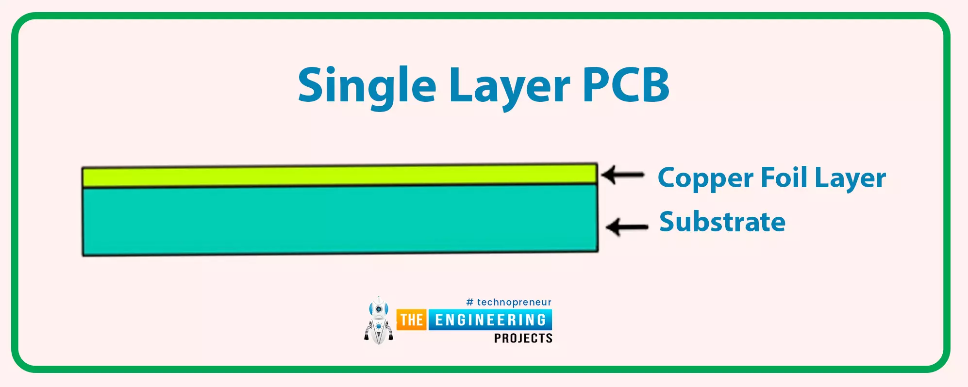
- Single-layer PCBs have only one conductive layer of copper.
- The PCB board itself has a total of 3 layers in single-layer PCB other than the copper layer which are substrate, solder mask, and silkscreen.
- In the past, phenolic aldehyde was used as a substrate but nowadays glass fiber epoxy resin is used because of its flexibility with temperature variations.

Single-layer Definition
- Single-layer PCB refers to a printed circuit board that has only 1 layer of conductive pattern.

- Single-layer PCBs are simple, low-cost and can be designed at home.
- Different materials like glass fiber reinforced epoxy resin with copper foil and a paper mask having phenolic resin with copper foil are used in the manufacturing of single-layer PCB.
Pricing of Single Layer PCB
Now let's have a look at the pricing of Single Layer PCB. As Single Layer PCB is the simplest form of PCB, so it's quite low cost as compared to other PCB types. Let's take the example of JLCPCB Fabrication House, a well-renowned PCB manufacturing company, that offers competitive rates for PCB designing.
- We need to open JLCPCB official site and click on its Order Now page, as shown in the below figure:
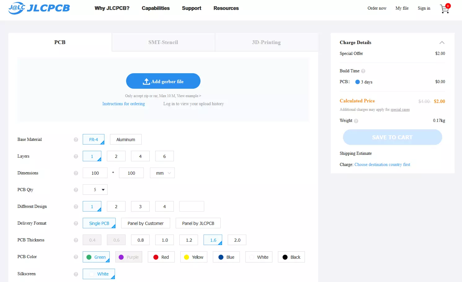
- As you can see in the above figure, I have selected 1 for Layers, so I am ordering for Single Layer PCB.
- The size of the Single Layer PCB is 100x100mm and I have placed the order for 5 pcs of PCB.
- For this order, JLCPCB has given me a price of $2.00, so you can see it's quite cheap to design Single Layer PCB.
Construction of single layer
- In 1950, the first single-layer PCB was designed.
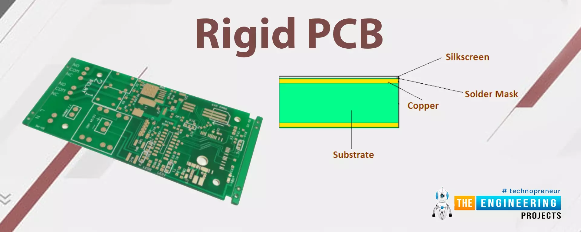
- The base material or substrate is made up of fiberglass and is compact in its sense.
- There is a copper layer that has conducting path for various competent on the boards above subtract. Needless to mention, different boards have different copper thicknesses consistent with your needs and demands, defined in ounces per sq. ft.
- On one hand, there is a solder mask layer on the top of the copper foil. The layer mainly protects the copper foil from insulating which avoids conduction in case direct contact happens with some conducting material.
- On the opposite hand, there's a silkscreen layer on the highest of all layers, which is especially in adding characters and symbols on the board, so it’s easy to have a far better understanding of the board.
Types of singles layer PCB
There are some types of single-layer PCB. We are going to explain them below concerning its manufacturing material.
- Single-layer rigid PCB
- Single-layer flexible PCB
- Single-layer rigid-flex PCB
- Single-layer high-frequency PCB
- Single-layer aluminum-backed PCB
1 Single-layer rigid PCB
- Single-layer rigid PCB is a type that is made up of a rigid material such as fiberglass.
- These PCBs are hard and prevent the circuit from bending and breaking.
- It's used in applications i.e. calculators, power supplies etc.
2. Single-layer flexible PCBs
- A single-layer flexible PCB has a flexible substrate like polyimide in its manufacturing.
- Single-layer flexible has so many advantages over single-layer rigid PCBs. But the cost is too high for its fabrication. A single-layer flexible PCB is shown below.
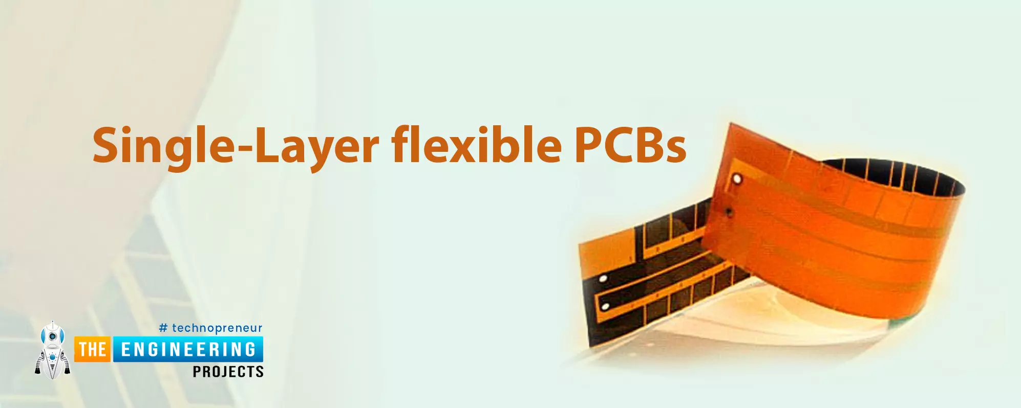
A single-layer flexible PCB
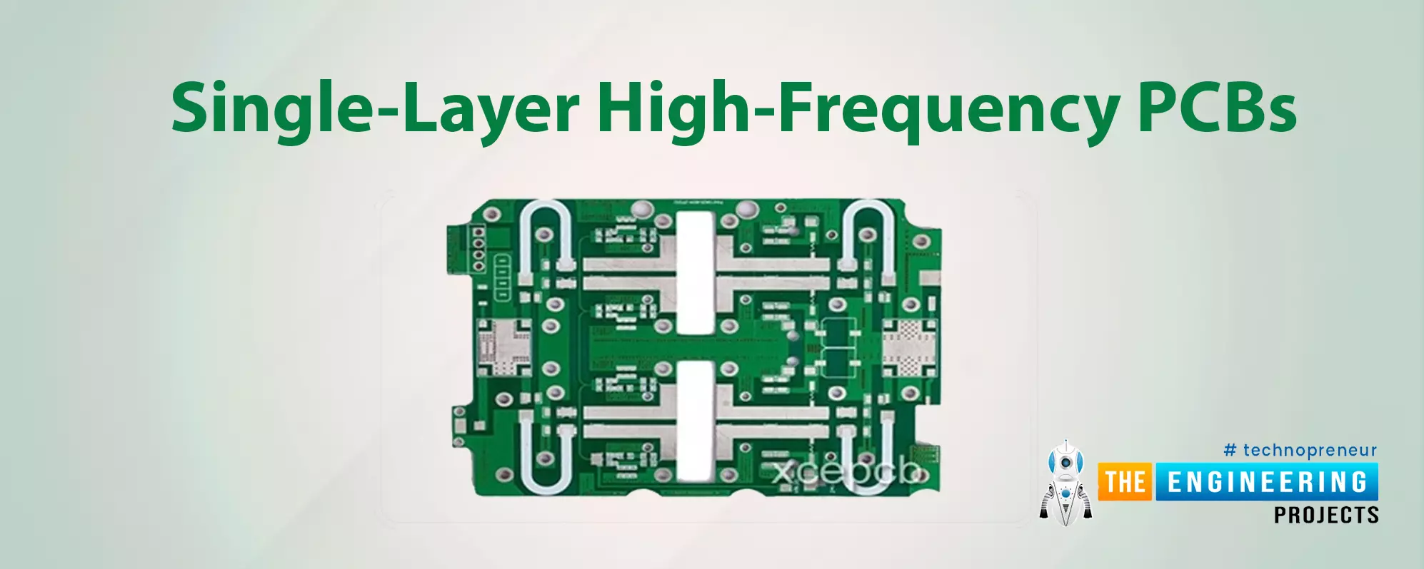
3. Single-layer high-frequency PCBs
- Circuits emitting a frequency in Gigahertz, single-layer high-frequency PCB is used.
- Polyphenylene oxide (PPO) or Teflon Material is used in single-layer high-frequency PCBs.
- If you are selecting High-frequency single-layer PCB, you should consider many aspects such as dielectric loss, thermal expansion, water absorption, etc.
- A single-layer high-frequency PCB is shown in the below figure
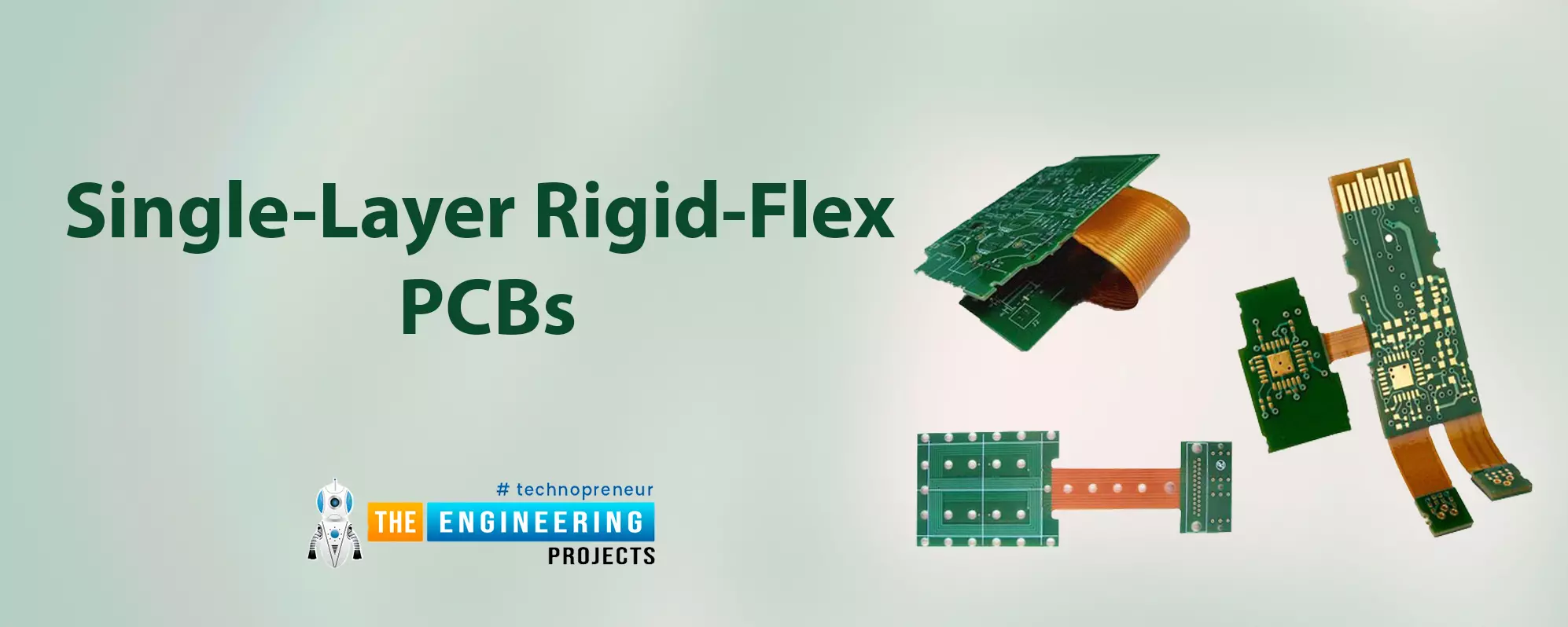
4. Single-layer rigid-flex PCBs
- Single-layer rigid-flex PCB is a combination of both Rigid PCB and Flexible PCB.
- Single-layer rigid-flex PCBs have so many advantages over single-layer rigid and flexible PCBs such as it reduces the size and weight of the overall PCB.
- Single-layer rigid-flex is shown below figure.
5. Single-layer aluminum-backed PCBs
- Single-layer Aluminium-backed PCB has an aluminum substrate.
- Aluminum-backed PCB is used with the thermal insulating material for the heat to dissipate by Aluminium.
- Single-layer aluminum-backed PCBs are shown below in Figure.
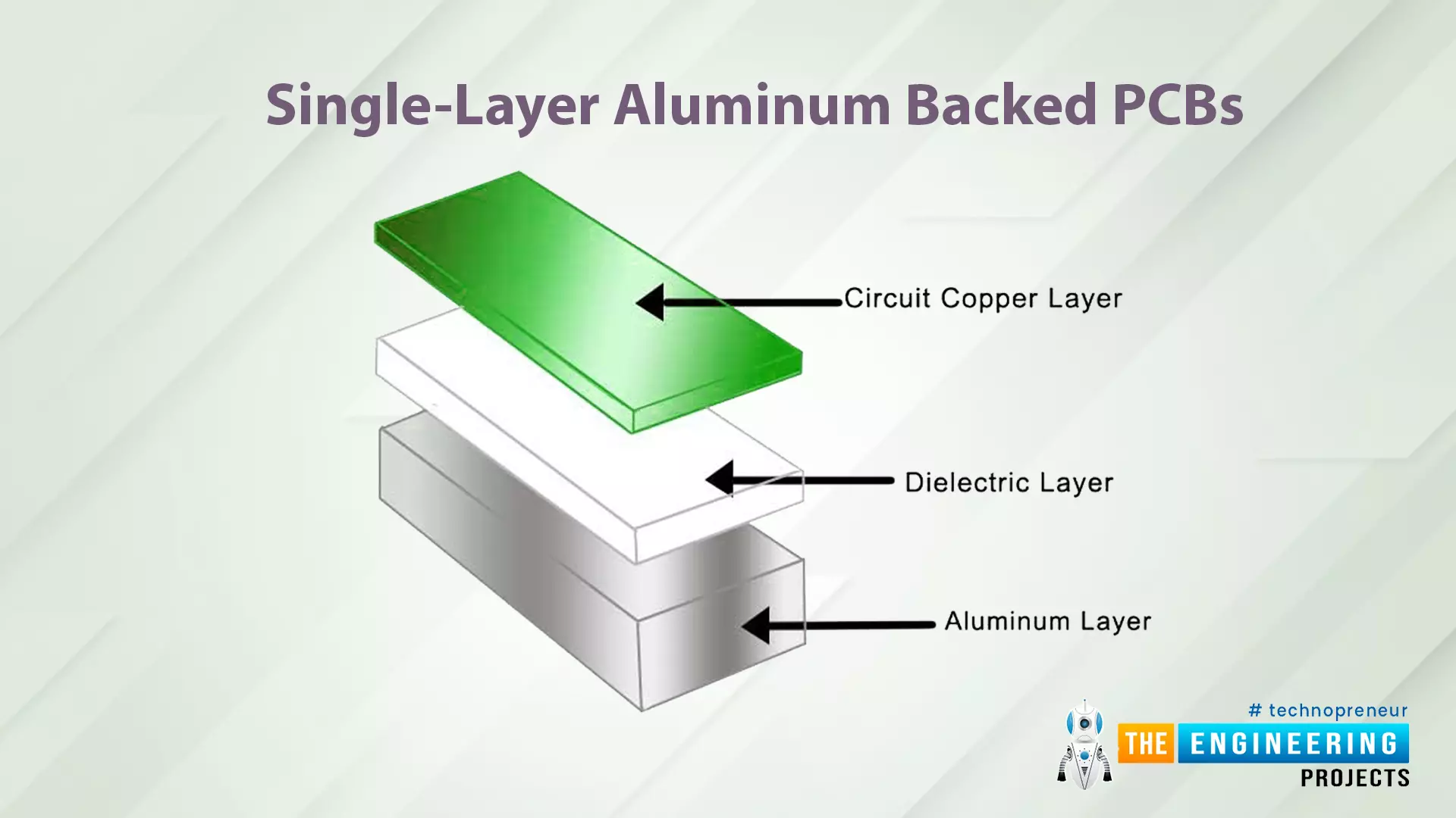
A single layer aluminum backed PCBs
Steps for the manufacturing process of PCB
- There are a lot of processes involved in the construction of a PCB.
- Almost 12-20 machines are used in the manufacturing of a simple single-layer PCB depending upon the demand of the customer and the requirement of the product.
- For ease of understanding, single layer PCB manufacturing process can be defined as
1. Cutting & Cleaning of PCB sheet:
- The circuit pattern is drawn on PCB using the photolithography technique in which warm iron is used to draw a pattern from photo paper to PCB.
- Photo paper is removed by washing PCB having photo paper on it.
- After drawing the pattern, check connecting nodes, jumpers, and docking points for additional components.
2. Etching with ferric chloride:
- prepare a solution of ferric chloride with water in a 1:3 ratio and dip board into it.
- The processing speed in this step is affected by the temperature of the solution and the thickness of the foil. You have to moderately heat the solution to speed up the process.
- Again clean the board with alcohol.
3. Drilling holes on the single layer PCB:
- now holes are drilled according to the requirement of the product. Clean the board again.
4. Soldering holes and lubricate sides of the board:
- at this stage, first of all, holes are soldered to make them able to make connections between components and layers.
- After soldering holes lubricating the sides of the board with a cover layer is done.
5. Testing of the final board:
- at this stage, the final prepared board is tested for whether it is ready or not.
6. Packaging:
- in the end, the final packaging is done and now the single layer PCB is ready to be delivered.

Common mistakes in single layer PCB manufacturing:
Following mistakes are made by designers during the manufacturing 9f the single-layer PCB.
1. incorrect conducting paths width:
- The maximum allowable width of the conducting path should be drawn to avoid voltage loss, overheating of the conductor, and low mechanical strength.
2. improper power circuit designs:
- When the width of the track is not made maximum then problems like output ripples, output voltage loss, and interference have to be faced. To avoid these problems track width should be maximum.
3. grounding problems:
- To avoid grounding problems, a separate insulating layer is used for wiring.
4. small gaps between copper:
- Gaps between copper conductors deposited on the board should not be so small, this can lead to the violation of the integrity of the board.
5. large no of holes on one plate:
- By increasing no of holes, no of conductive paths increases, and this, in turn, increases resistance.
Application for single-layer PCB
It is no doubt that single-layer PCBs are very simple. But single layer PCBs are used still in such a lot of complex devices. Some devices are listed below.
- Single-layer PCBs are used in digital cameras circuits.
- Single-layer PCBs used in coffee-making machine circuits.
- Single-layer PCBs are used in soiled state drives which are mostly used in the power industry.
- Single-layer PCBs are utilized in switching relays which are mostly utilized in the automotive and power industry.
- Single-layer PCB used in vending machine circuits.
- Single-layer PCBs used in digital calculators which are consist of only a single PCB.
- Single-layer PCB used in photocopy and printer machine circuits.
- Single-layer PCB is used in radio and stereo equipment circuits.
- Single-layer PCB is utilized in digital microwave timer circuits to modify on or off the oven timely.
- Single-layer PCB is used in led lighting circuits for making power light circuits.
- Single-layer PCB used in digital and analog power supplies circuits.
- Single-layer PCB used in surveillance machine circuits.
- Single-layer PCBs are used in sensors products circuits.
- Single-layer PCBs are used in packing machines to achieve the high targets of fast-packing and are mostly used in packing industries.
- Single-layer PCBs are used in timing circuits to switch on or off the machine timely.
Advantages of single-layer PCB
There are some advantages given below of single-layer PCB.- The single-layer PCs is very easy to design and has a lower probability to make incorrect design because the single-layer PCBs is very simple.
- Its price is very less especially when it is ordered in bulk quantity as compared to the other types of PCBs.
- It is easy to understand for anyone because it is a very simple circuit
- Because its components are installed on only one side there for its a required lower jumper o compensate for the circuit.
- Its drilling, soldering, de-soldering, and components inserting process is very easy because single layer PCBs only consist of a single layer.
- Its design circuit required a very short time to make a simple design.
- There is less probability of short-circuiting and producing noise because its components are installed at some distance from each other.
- For fault tracing and repairing of this single layer PCB need less time.
- When we compare the single-layer PCBs to the other types of PCBs. It is more reliable and efficient.
- The installation of single-layer PCBs is very easy.
Disadvantages of single layer PCB:
- Single-layer PCBs have many advantages regarding cost, efficiency, and ease of installation but they still can not be used for any circuit because of their limitations. The limitations or disadvantages of using single layer PCB are discussed below:
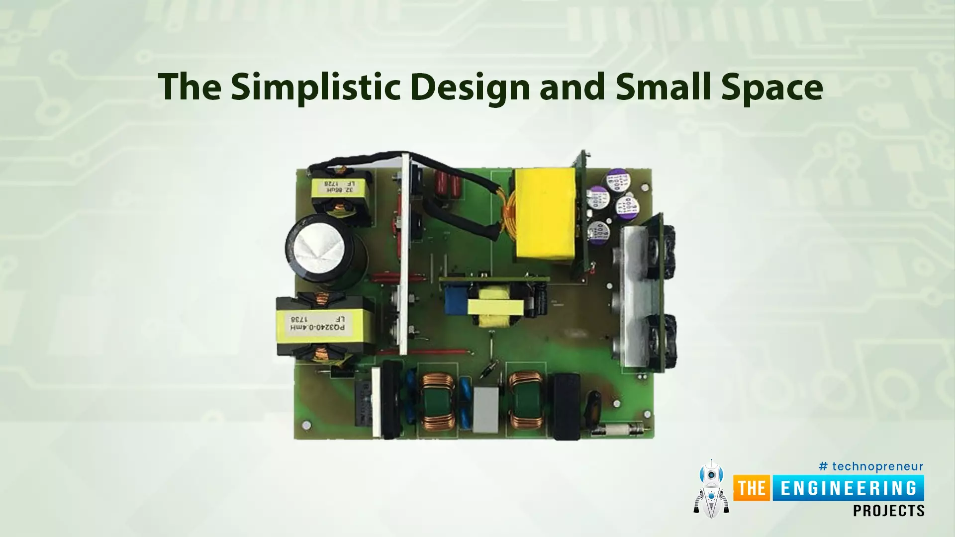
The simplistic design and small space:
- Single-layer PCB has a very simple design and this simplistic design presents as the hurdle in complex devices that require a lot of components and connections.
- To mount a large no of components, large space is required but single layer PCBs don’t have enough space to mitigate this problem.
Slow speed and low operating capacity:
- As they have a limited no of components so their speed is slow, their power is also slow.
- Due to their low speed, they have low operating capacity.
Large size and high weight:
- To add components to the single-sided PCB you need to enhance PCB into its dimensions. As it is single-sided so that’s why we can not add layers. By enhancing PCB into its dimensions, the size of PCB.
- The enhanced size and large no of components ultimately enhance the weight of single-layer PCB.
Conclusion:
- At the end of it all, we can conclude that single-layer PCBs have unique advantages, benefits, and applications but as an end-user, you always have to choose which type of PCB you need.
- In modern technology advancements, single-layer PCBs are now in an underestimated situation but are still used.
- With a low budget and volumes of specific design single-layer PCB is the right choice when compared to the other types of PCB.
That’s all for today’s article. I hope you have enjoyed the article and made grip on the understanding points. However, if you still face any skepticism regarding single-layer PCB then please feel free to leave your questions in the comment section. I will provide an answer to these questions to the best of my knowledge and research skills. Also, provide us with your innovative feedbacks and suggestions you improve the quality of our work and provide you content according to your needs and expectations. Stay tuned! Thank you for reading this article.