How to use ADC with STM32?


An Analog to Digital Converter (ADC) converts a continuous signal (usually a voltage) into a series of discrete values ??(sequences of bits). The main features are:
- Resolution (in analog terms): It is the minimum variation of the analog input voltage that can determine the variation of the LSB, that is of the least significant bit of the output code. Since the quantization step Q corresponds to the LSB, it can be said that the resolution coincides with the quantization step Q (and therefore is measured in Volts). We can say that the quantization step Q corresponds to the LSB because two contiguous quantization bands, each of amplitude Q, are identified by codes that differ only for the least significant bit.
- Resolution (in digital terms): It is the number n of bits present at the converter output, that is the number of bits with which the converter encodes a sample of the analog input signal. As the number of bits of the converter increases, the number of quantization bands increases and (with the same full-scale value VFS) their amplitude decreases, an amplitude which is nothing more than the step Quantization Q. If the quantization step narrows, the smaller the voltage variation necessary to determine the variation of the LSB, i.e., of the least significant bit of the code, becomes the exit. So, saying that a converter has many bits is equivalent to saying that the voltage variation necessary to make the LSB vary is small. The image below shows the 3 bits ADC input-output characteristics.
- Full-scale voltage: It is the range, that is the maximum excursion, of the input voltage. Typical dynamic values are between 10 Vpp ( pp peak to peak) and 20 Vpp, unipolar or bipolar.
- Types of response: in general, ADCs have a response of a linear theoretical type of response, but there are also types with a logarithmic response.
- Accuracy: indicates the goodness of the conversion depends on it. The error made by the ADC is usually measured. This error consists of two components: a quantization error and a non-linearity error.
- Sampling frequency: A sampling is an operation with which the input signal is discretized over time, transforming it into a succession of values, samples in fact, which will subsequently be digitized. The simplest way to extract values is to use a switch, in series with the signal, which closes and opens at defined and equidistant intervals. The smaller this interval, called the sampling step (Ts), the more faithful the reconstruction of the signal will be starting from its samples. Likewise, too small a sampling step leads to a waste of resources (measurement time, memory for data storage). A sampling of the signal generally indicates not only its discretization over time but also its maintenance until the next closing of the circuit-breaker. These two phases are realized by special circuits called Sample & Hold (S / H).
There are different types of ADCs, the most common are listed below (illustrating their operation is not the purpose of this article):
- A direct conversion ADC (Flash ADC)
- A Successive Approximation Register (SAR) ADC
- One dual ramp ADC (Dual Slope or integration)
- A pipeline ADC
- A tracking ADC (delta-coded)
Generally, STM32 microcontrollers have at least one ADC (a SAR ADC) with the following characteristics:
- Resolution: ADCs have a resolution of up to 12 bits with a maximum conversion frequency of 2.5 MHz, with 18 multiplexed channels among which 16 can be available for measurements of external signals, the other two are for internal measurements (temperature and voltage).
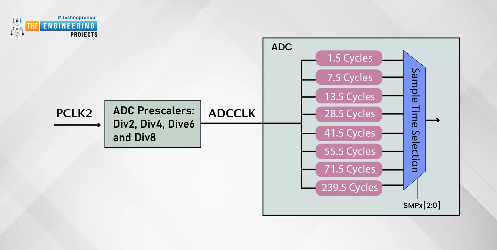
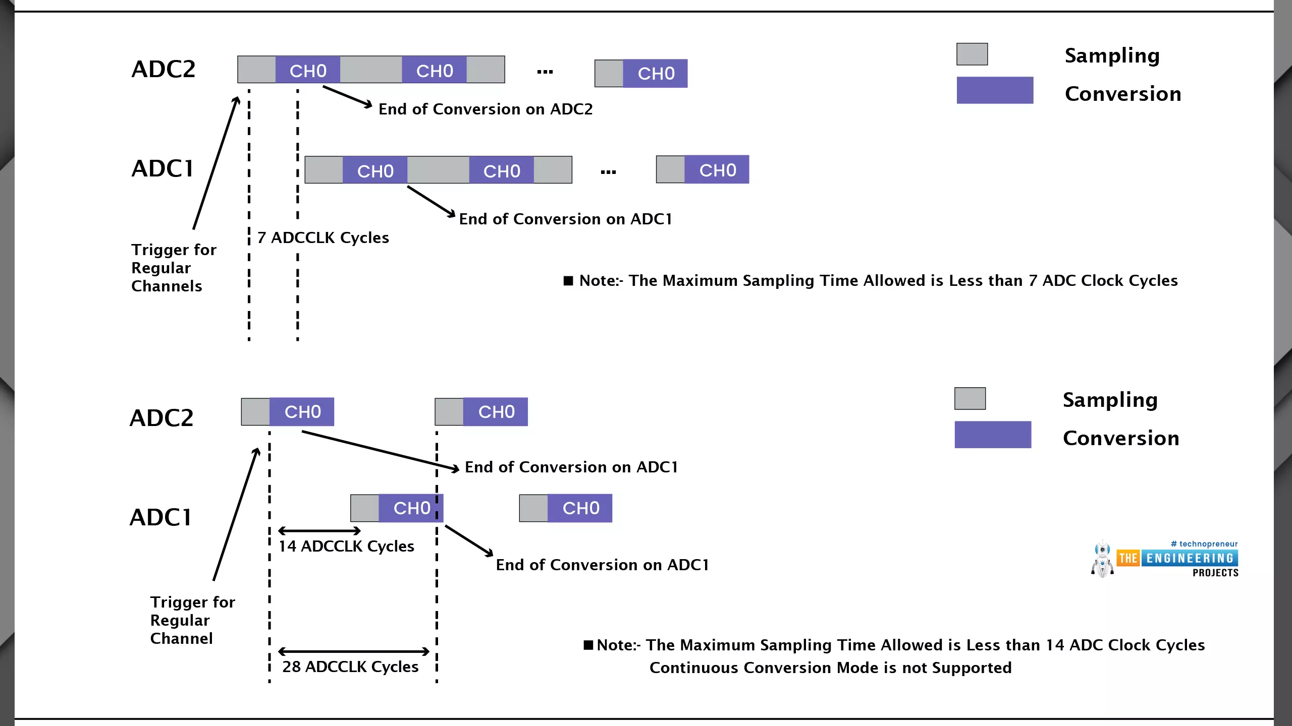
- Conversion Time and Conversion Groups: The conversion time can be individually programmed for each channel. There are 8 discrete times conversions for each ADCCLK clock frequency (Fc), these times range from 1.5 to 239.5 cycles.
Fc = ADCCLK / (12.5 + Number of cycles)
Each ADC has two conversion modes: “regular” and “injected”.
- The "regular" mode allows you to specify a channel or a group of channels to be converted in turn one after the other. The conversion core can consist of more than 16 channels, and the order in which the channels must be converted can also be programmed. The conversion can be initiated by software or by a hardware event consisting of a series of timer signals or by line 1 of the EXTI. Once the conversion has started, you can carry out continuous conversions, or you can operate discontinuously by converting a selected number of channels and then stopping the conversion pending the triggering of the next core. At the end of a conversion the result is stored in a single register (result register) and an interrupt can be generated. The ADC1 has a dedicated DMA channel that can be used for transferring the converted value from the result register to a memory buffer. Through this method, an entire conversion cycle can be copied into memory, eventually obtaining a single interrupt generated by the DMA. To further speed up the conversion, a double-sized buffer can be used to generate two interrupts: one when the first half has been filled (first conversion cycle) and the other when the second half is filled (second conversion cycle). This mode can be combined with the "DMA circular buffer mode" to handle multiple conversions with hardware.
- The second conversion mode is called the “injected group”. It is able to carry out the conversion sequence up to a maximum of four channels, which can be triggered by a software or hardware event. Once triggered, it will stop the conversion of the regular group, carry out its sequence of conversion and then will allow the regular group to continue the conversion. A conversion sequence can be configured in this mode. Unlike the regular group, in this mode, each result has its own register (result register) and its own offset register. This last register can be programmed with a 16-bit value automatically deducted from the ADC result.
Furthermore, the "Dual Conversion Modes" can be active:
In the STM32 with almost two ADCs and it is, therefore, possible to perform different conversion modes: in these types of conversion the ADC2 acts as a slave while the ADC1 acts as a master allowing 8 different types of conversion.
- Injected Simultaneous Mode and Regular Simultaneous Modes: These two modes synchronize the regular and injected group conversion operations on two converters. This is very useful when two quantities (current and voltage) have to be converted simultaneously.
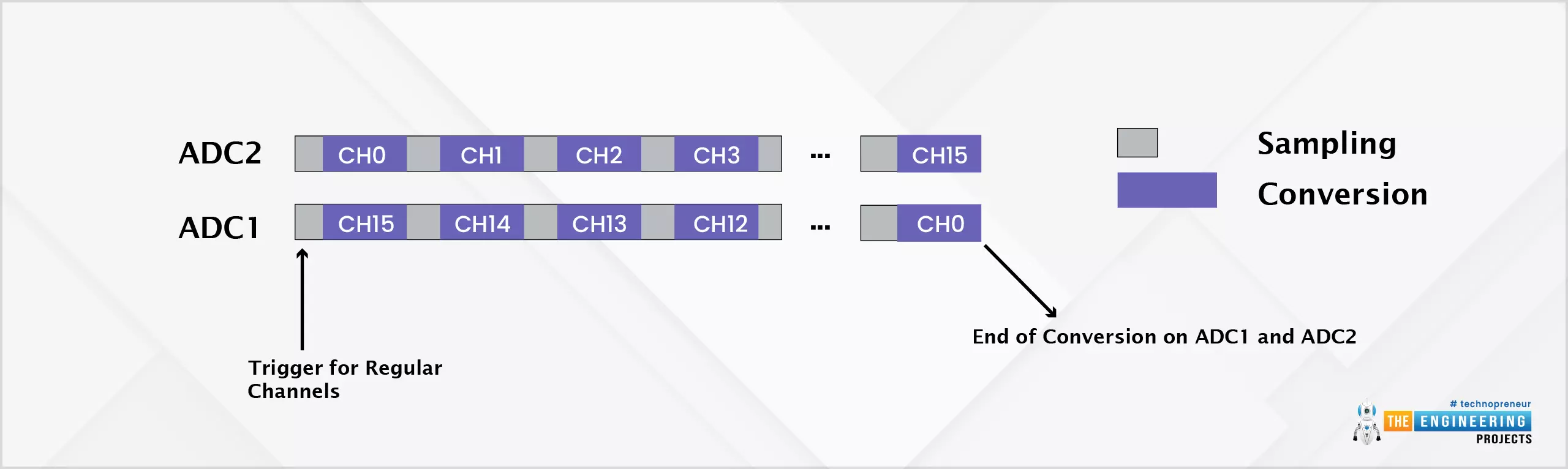
- Combined Regular / Injected Simultaneous Mode: This mode is a combination of both the regular and injected modes and allows us to have a synchronized conversion sequence.
We are now ready to write a first simple example using the ADC peripheral. The goal is to measure the voltage in a voltage divider composed of a fixed value resistor and a potentiometer (so that by moving the potentiometer cursor, the voltage to be read varies) we begin by configuring our peripheral with STCube Tool. For this project, we will use the NUCLEO STM32L053R8. This board has only one ADC with 16 channels and a resolution of up to 12bit.
Now we’ll see the configuration step by step:
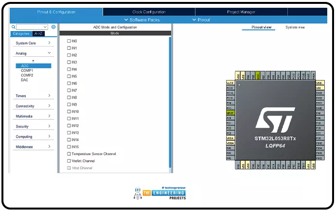
ADC channel selection
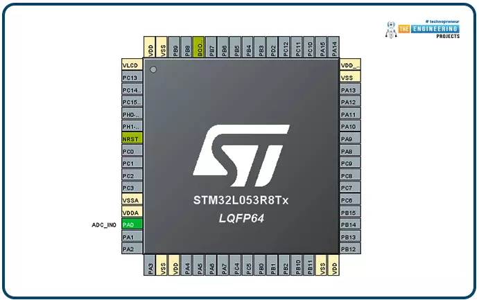
We have to flag IN0 to activate Channel 0, then we can configure the peripheral. Channel 0 is on GPIO PA0 as we can see in the picture below:
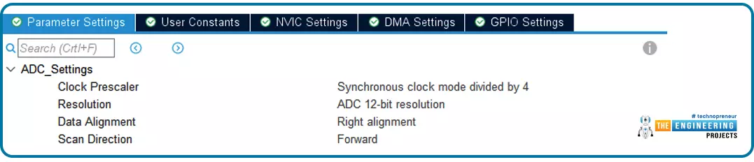
ADC setting
We select the ADC_prescaler equal to 4, resolution to 12bit (maximum of a resolution, we can choice between 6, 8, 10 and 12 bits), “right data alignment” (we can choose between right and left alignment), and “forward” as scan direction (we can choose between forward and backward).
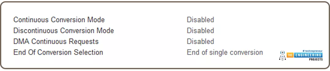
For this first example we’ll hold disabled Continuous, Discontinuous conversion and DMA mode. Furthermore, the ADC sets, at the end of single conversion, the EoC (End of Conversion) flag.
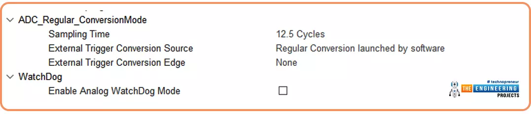
ADC Regular conversion mode
We select 12.5 Cycles as sampling time (in this way the sampling frequency is 320 kHz obtained from the formula described above), the start of conversion is triggered by software. Furthermore, for this application the watchdog is disabled.
After the generation of the initialization code with STCube, we can find in our project the ADC configuration. As for every peripheral, the HAL library defines the dedicated C structure, for the ADC defines “ADC_HandleTypeDef”.
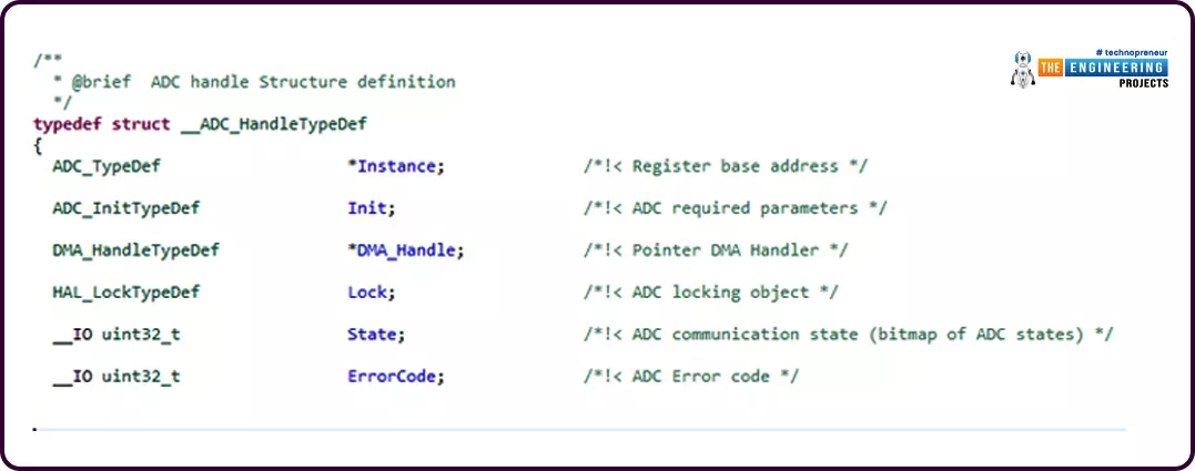
In our case the “ADC1” is the instance that points to our ADC. The structure “ADC_InitTypeDef” is used to handle the configuration parameters. In our example is generated as follow:
static void MX_ADC_Init(void) { /* USER CODE BEGIN ADC_Init 0 */ /* USER CODE END ADC_Init 0 */ ADC_ChannelConfTypeDef sConfig = {0}; /* USER CODE BEGIN ADC_Init 1 */ /* USER CODE END ADC_Init 1 */ /** Configure the global features of the ADC (Clock, Resolution, Data Alignment and number of conversion) */ hadc.Instance = ADC1; hadc.Init.OversamplingMode = DISABLE; hadc.Init.ClockPrescaler = ADC_CLOCK_SYNC_PCLK_DIV4; hadc.Init.Resolution = ADC_RESOLUTION_12B; hadc.Init.SamplingTime = ADC_SAMPLETIME_12CYCLES_5; hadc.Init.ScanConvMode = ADC_SCAN_DIRECTION_FORWARD; hadc.Init.DataAlign = ADC_DATAALIGN_RIGHT; hadc.Init.ContinuousConvMode = DISABLE; hadc.Init.DiscontinuousConvMode = DISABLE; hadc.Init.ExternalTrigConvEdge = ADC_EXTERNALTRIGCONVEDGE_NONE; hadc.Init.ExternalTrigConv = ADC_SOFTWARE_START; hadc.Init.DMAContinuousRequests = DISABLE; hadc.Init.EOCSelection = ADC_EOC_SINGLE_CONV; hadc.Init.Overrun = ADC_OVR_DATA_PRESERVED; hadc.Init.LowPowerAutoWait = DISABLE; hadc.Init.LowPowerFrequencyMode = ENABLE; hadc.Init.LowPowerAutoPowerOff = DISABLE; if (HAL_ADC_Init(&hadc) != HAL_OK) { Error_Handler(); } /** Configure for the selected ADC regular channel to be converted. */ sConfig.Channel = ADC_CHANNEL_0; sConfig.Rank = ADC_RANK_CHANNEL_NUMBER; if (HAL_ADC_ConfigChannel(&hadc, &sConfig) != HAL_OK) { Error_Handler(); } /* USER CODE BEGIN ADC_Init 2 */ /* USER CODE END ADC_Init 2 */ }The function HAL_ADC_MspInit(ADC_HandleTypeDef* hadc) needs to initialize the peripheral and define the clock and the GPIO ( in our case PA0).
void HAL_ADC_MspInit(ADC_HandleTypeDef* hadc) { GPIO_InitTypeDef GPIO_InitStruct = {0}; if(hadc->Instance==ADC1) { /* USER CODE BEGIN ADC1_MspInit 0 */ /* USER CODE END ADC1_MspInit 0 */ /* Peripheral clock enable */ __HAL_RCC_ADC1_CLK_ENABLE(); __HAL_RCC_GPIOA_CLK_ENABLE(); /**ADC GPIO Configuration PA0 ------> ADC_IN0 */ GPIO_InitStruct.Pin = GPIO_PIN_0; GPIO_InitStruct.Mode = GPIO_MODE_ANALOG; GPIO_InitStruct.Pull = GPIO_NOPULL; HAL_GPIO_Init(GPIOA, &GPIO_InitStruct); /* USER CODE BEGIN ADC1_MspInit 1 */ /* USER CODE END ADC1_MspInit 1 */ } } /** * @brief ADC MSP De-Initialization * This function freeze the hardware resources used in this example * @param hadc: ADC handle pointer * @retval None */The function HAL_ADC_MspDeInit(ADC_HandleTypeDef* hadc) needs to de-initialize the peripheral.
void HAL_ADC_MspDeInit(ADC_HandleTypeDef* hadc) { if(hadc->Instance==ADC1) { /* USER CODE BEGIN ADC1_MspDeInit 0 */ /* USER CODE END ADC1_MspDeInit 0 */ /* Peripheral clock disable */ __HAL_RCC_ADC1_CLK_DISABLE(); /**ADC GPIO Configuration PA0 ------> ADC_IN0 */ HAL_GPIO_DeInit(GPIOA, GPIO_PIN_0); /* USER CODE BEGIN ADC1_MspDeInit 1 */ /* USER CODE END ADC1_MspDeInit 1 */ } }
Before describing the code let's see how to make the connections on the development board.
We need a 10kOhm potentiometer and a 2kOhm resistor. The potentiometer is connected between 3.3V and 2kOhm resistor, the common point is connected to PA0, and finally, the other end of the 2k Ohm resistor is connected to the ground pin.
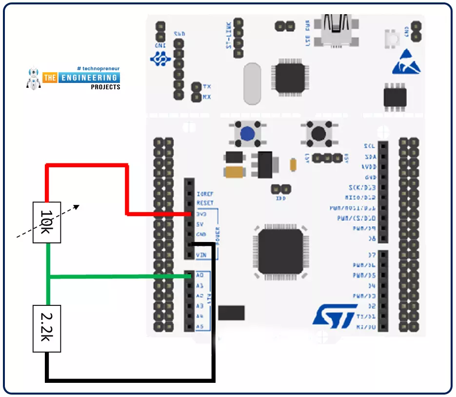
Acting on the potentiometer we will see the read voltage vary from 3.3 Volt to about 0 Volt.
Now let's dive into the code: In the Includes section we add the header file of main./* USER CODE END Header */ /* Includes ------------------------------------------------------------------*/ #include "main.h" /* Private includes ----------------------------------------------------------*/ /* USER CODE BEGIN Includes */ /* USER CODE END Includes */
In “Private variables” section we find “ADC_HandleTypeDef hadc” as previous said is an instance to C structure to handle the ADC peripheral. Then, we add three variables:
- Resolution defines the number of steps used by ADC (12bit = 2^12 -1= 4095) is a constant integer;
- vs defines the maximum voltage to read, is a constant float;
- volt is the variable where the voltage value read by the ADC is store ( is a float variable)
/* Private variables -----------------------*/ ADC_HandleTypeDef hadc; /* USER CODE BEGIN PV */ const int Resolution = 4095; const float Vs =3.300; float volt; /* USER CODE END PV */
Then, we can find the protype of function to handle the peripherals and resources initialized (system timer, GPIO, and ADC).
/* Private function prototypes -----------------*/ void SystemClock_Config(void); static void MX_GPIO_Init(void); static void MX_ADC_Init(void); /* USER CODE BEGIN PFP */ /* USER CODE END PFP */
Finally, the main starts.
In the first part we call functions to initialize the peripherals and resources used:
int main(void) { /* USER CODE BEGIN 1 */ /* USER CODE END 1 */ /* MCU Configuration--------------------------------------------------------*/ /* Reset of all peripherals, Initializes the Flash interface and the Systick. */ HAL_Init(); /* USER CODE BEGIN Init */ /* USER CODE END Init */ /* Configure the system clock */ SystemClock_Config(); /* USER CODE BEGIN SysInit */ /* USER CODE END SysInit */ /* Initialize all configured peripherals */ MX_GPIO_Init(); MX_ADC_Init(); /* USER CODE BEGIN 2 */ /* USER CODE END 2 */ /* Infinite loop */ /* USER CODE BEGIN WHILE */
In the second part, that is, inside an infinite loop (while (1)) there is the function to start the conversion of the ADC, read the data and save it in the variable volt and finally stop the conversion wait for a second and start with the conversion and so on.
while (1) { /* USER CODE END WHILE */ HAL_ADC_Start(&hadc); if(HAL_ADC_PollForConversion(&hadc,10)==HAL_OK) { volt=HAL_ADC_GetValue(&hadc)*Vs/Resolution; } HAL_Delay(1000); HAL_ADC_Stop(&hadc); /* USER CODE BEGIN 3 */ } /* USER CODE END 3 */ }
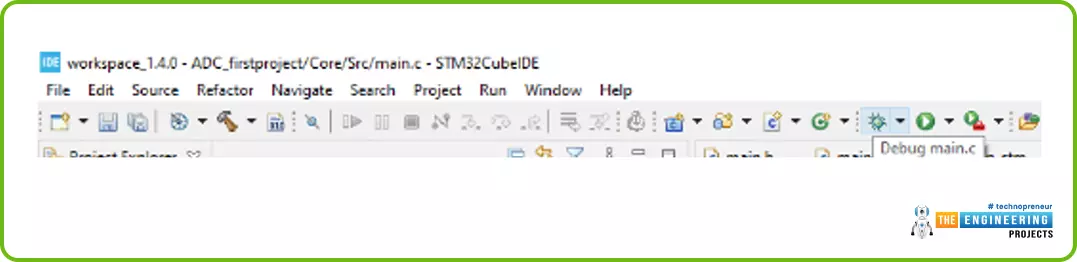
Now, once our code has been compiled, we can debug it in real-time, just press the "spider" icon (see figure below) and see how the volt variable varies by acting on the potentiometer.
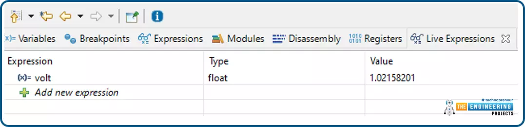
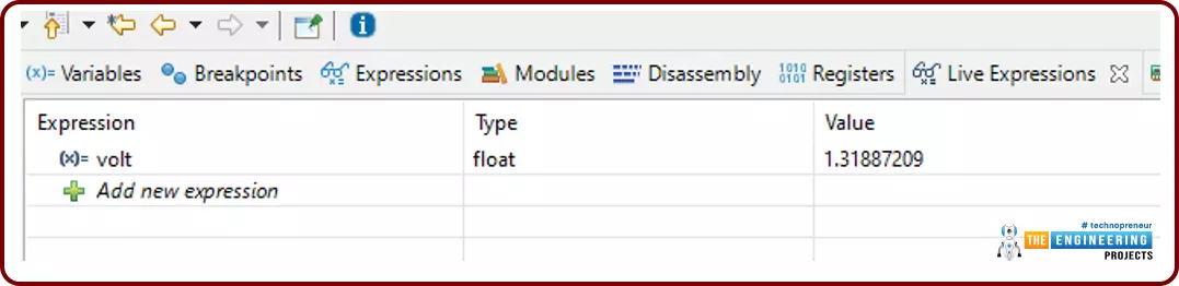
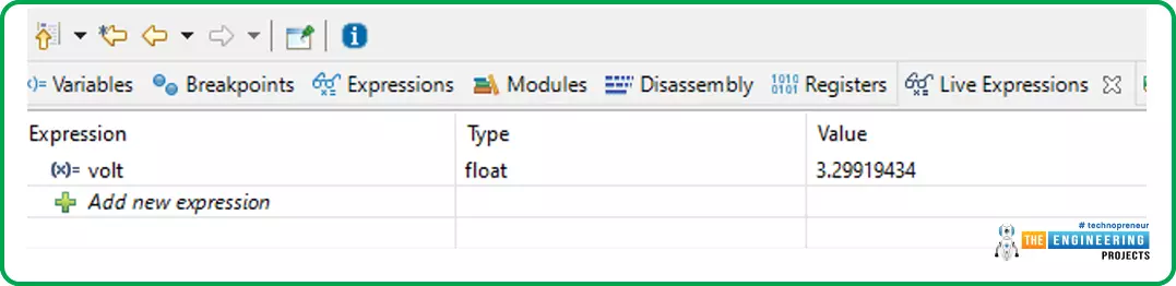
Once we have clicked on the debug button, at the top right, we can select the "live expression" window and add (by writing the name in the table) the variable to be monitored.
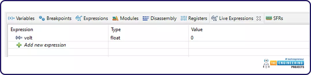
Now we can start the debug by clicking on the “Resume” button (on the top right) or by pressing the F8 key (on our keyboard).
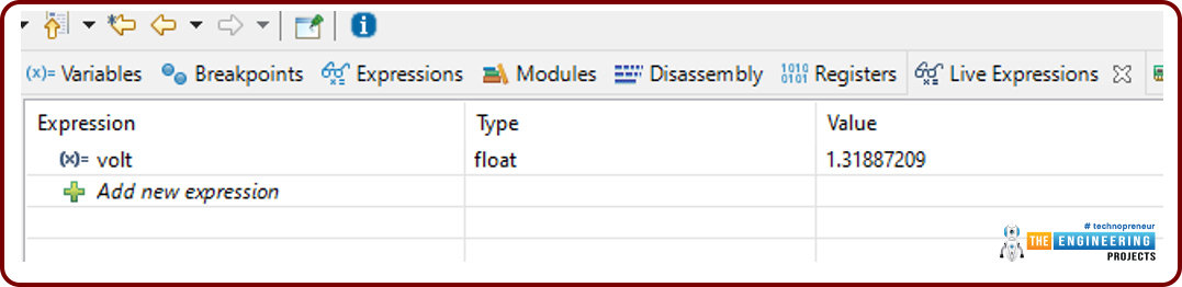
We are now ready to read our voltage value. We will see that by acting on the potentiometer we will read the voltages in the whole range considered.
Some measures are shown below:
- First reading volt=1.3188 Volt
- First reading volt=3.29919 Volt
- First reading volt=1.02158 Volt