Introduction to High-Speed PCB Design


Hello everyone and welcome to this article which will be a great introduction to high-speed PCB design. For sure it is going to be a very interesting class. Let me start by posing a question; Is this something that you have ever come across in your world of PCB design? Where you spent too much time doing the schematics, selecting the right components, doing the footprint addition, generating the netlists, doing the proper layout and routing and sending the end product of your design to the manufacturer? At this level you might probably be designing standard types of PCB boards and if someone was to introduce a project that talks about signal integrity, reflections or even crosstalk, very much believe you will feel like a lost person. It might be something new to you. The reason is that such kind of task is not what you have been handling in your day-to-day design activities.
In this field of PCB design, you might not guess what your clients want in the future and sooner or later, you might be slapped with a design that involves high-speed PCB design process and at this stage be assured of finding things so hard if you have never worked with the high-speed PCB designs. Today we are going to have a look at the high-speed PCB design and this article is best suited for people who want to go beyond the horizon when it comes to printed circuit board design.
What is a high-speed PCB design?
When we introduce a high-speed PCB design, signal integrity should be the first thing that runs in your mind. When your signal integrity starts to be affected by the physical properties of your printed circuit board like the schematic, layouts etc then the design of your board is a high-speed PCB design.
Signal integrity is a set of measures that define electrical signal quality.

- When you complete the design of your PCB boards and you come across challenges such as attenuation, reflections, delays, crosstalk and so on, the feel at home and welcome to the field of high-speed PCB design.
- The amount of attention paid to these arising challenges is what makes the High-speed PCB design very unique.
- You might have been used to the design of easy boards where your focus is only on the placement of components and routing but sometimes you will come across a design that where you place your components is very important, the way you do the routing, the distance between different signals must be considered, where you place your traces and which type of components should be interconnected
- If you take all these precautions then expect a very new different type of PCB design. You will be having a whole new experience in your design work.
Having introduced what high-speed PCB design is and making note that it is all about signal integrity, now let us have a look at the signal integrity to get a proper understanding;
How to place an order for High-Speed PCB?
There are many online PCB companies, that offer High-Speed PCB designing. For this tutorial, let's take the example of PCBWay, a China-based PCB Fabrication House, that offers competitive prices for PCB designing. So, let's take a look at how to place a High-Speed PCB order on PCBWay:- First, create a new account on the PCBWay official site.
- Click on the PCB Instant Quote tab and a PCB Calculator will open up.
- Here, click on the Advanced PCB Button at the top and you will get the calculator as shown below:
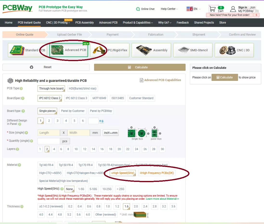
- As you can see in the above figure, I have selected High Speed in the Materials section.
Brief on signal and signal integrity:
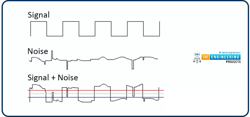
When doing a PCB design of any kind, it is obvious that you will be sending some sort of signal through copper traces from the input to your desired area of interest. The signal you will be sending can either be a digital signal or an analog signal.
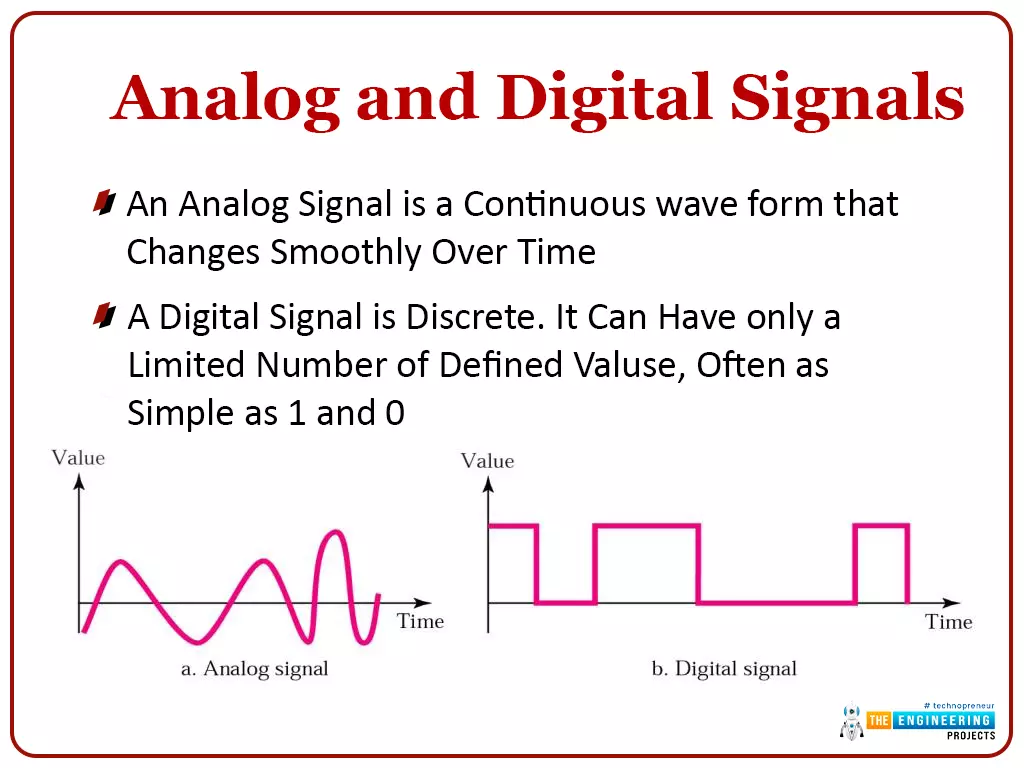
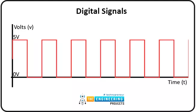
Digital signals
- Also referred to as the square signal and it is the output that you will always come across any digital signal that exist in this planet.
- Unlike in the analog signal which has random numbers spread all over, the digital signal has a well-organized system of outcomes represented by a high and a low point or a 1 and a 0 or even some refer to them as an off and an on.
- Let us look at the figure below which is an indication of a digital signal.
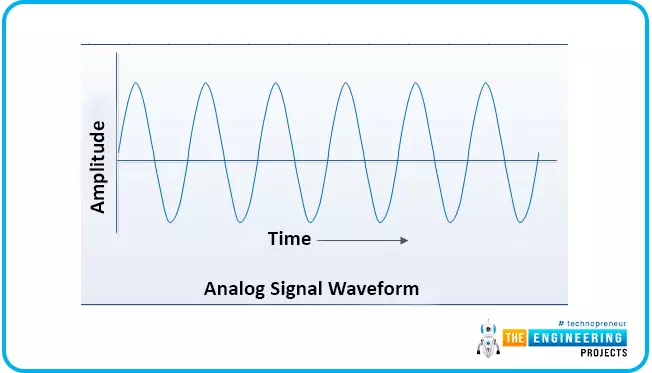
Analog signals
- This type of signals has random points of output which are made up of both negative and positive values.
- Unlike the digital signal that has on and off points, the analog signals have random results that are defined by there frequencies and the signal strength.
- The following is the output you should expect when using the analog signals.
The main issue about these signals is that they are prone to interference and this is where we bring in signal integrity because anytime a signal is affected by the environment there are some issues that arise.
Let us have a look at the following example.
Let us say you have a circuit that is transmitting signal from point 1 to point 2 in your PCB board. The point 1 can be classified as the transmitter and point 2 can be classified as the receiver. As the signal moves from point 1 to point 2, there is a likelihood that the signal is affected by different factors like;
- Signal ringing; this occurs when there is unwanted shifting of current or voltage which will lead to the flowing of extra current in your trace hence delaying the arrival of the signal.
-
- Signal reflection; this is when your signal is flowing in your coper traces but the whole signal does not get to the destination since some of it is reflected back to the origin.
- Signal noise; this occurs when there is a random fluctuation of signals in your board which in turn affects the signals that are close to it. The fluctuation may end up damaging the signal data being transferred in your board.
- Signal timing; some times when you send your signal through your copper traces, they do not get to that destination in time so that it can match with the clock signals. When this happens the signal might be interpreted as a zero while in actual sence it wss one. This is called signal timing.
- Signal crosstalk; this occurs when you place two copper traces too close to each other whle the traces carry different signals. The electromagnetic radiation that canoriginate from one signal might affect the other sisgnal hence corrucpting the data flowing in it.
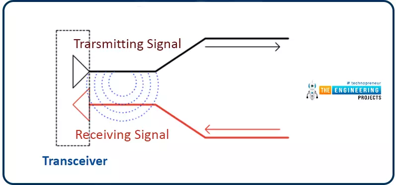
Remember that the listed challenges above are just some of the challenges that you might come across during the design of the PCB. Otherwise, we have so many others that we have not mentioned above and all of them just have one thing in common which is causing of disturbance to the signal you are sending from point 1 to point 2.
- Anytime the signal path is disturbed, the integrity of the data being send is corrupted and therefore, your work as a high speed PCB designer is to ensure that the integrity of the signals is protected at all cost.
- The signal should leave point 1 with a particular wave form and it should arrive at the destination which is point 2 with the same wave form and all the data intact.
How to determine if the project is high speed.
In reality, there is no a specific way to determine if the project is a high speed PCB project or not but the evaluation should be done by case to case. As we have noted in our example above, the first thing that should indicate that your project is classified as a high speed project is when you come across some signal integrity challenges in your PCB layout process.
You can identify a high speed design PCB by;
- Some specific device designs involve high speed PCB design. Some of them are designing of cell phone boards, motherboards and DSL routers are classified as high speed design projects. If you will be using specific technologies such as HDMI, SPI, UARTS, I2C and USB, just know that you will be dealing with the high speed projects.
- When the digital frequency is equal or more that the 50MHz.
- When the PCB board being designed has a very small size and the location of the components to be place creates a huge challenge to the designer.
- The main circuit is made up of so many subcircuit that are connected to each other by the use of very high speed interfaces such as the DSI and the CSI.
High speed PCB design Big Three Problems.
When working on the high speed PCB design, there are a number of issues that you will come across while trying to transmit your signal from point 1 to pint 2 and the main three challenges that you are likely to encounter are;
Integrity
Here we have to look at our signal at the destination and ask ourselves if the signal looks exactly as it should look like. If the signal does not look like it should, then it must have faced some interferences along the way which might have ruined its integrity.
Noise
The issue here is if your signal came across any form of interference during the transmission. It is obvious that PCB signals have some sought of noise in their output, but if this noise exceeds a certain limit, it might corrupt the signals being transmitted.
Timing
We are looking at how the signals are arriving at the destination. Are they arriving at the expected time with respect to other signals? Remember that all the signals in a PCB board are controlled by the clock and if the transmitted signal does not match with the clock signal then the signal is corrupted.
Correcting the Big Three Problems
The big three problem can be rectified by involving the following three solutions;
Matching
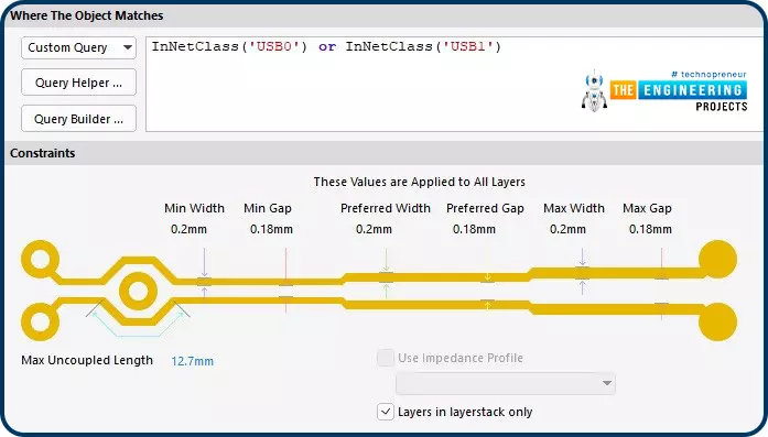
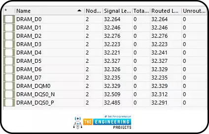
If traces have a matched length, it will ensure that the signals arrive at the same time and sync with the rates of the clock. Matching is a must thing when working with HDMI, SATA, USB, PCI Express and the DDR.
Spacing
The close you place your traces to each other, the more they are prone to noise and other forms of interferences. Therefore, it is advisable to ensure that your traces are having proper standard spacing. By placing your traces where they should be, with proper spacing reduces the amount of noise affecting your trace.
Impedance
By ensuring that you have proper impedance between your receiver and the transmitter will create a direct effect on the quality od the signal and its integrity. This will also have an impact on how your signals are exposed to the noise challenge.
Design rules and challenges for high speed design.
As it is in any engineering design work, there are rules that have to be followed when we are handling the high speed PCB design. Let us have a look at some of these challenges in depth;
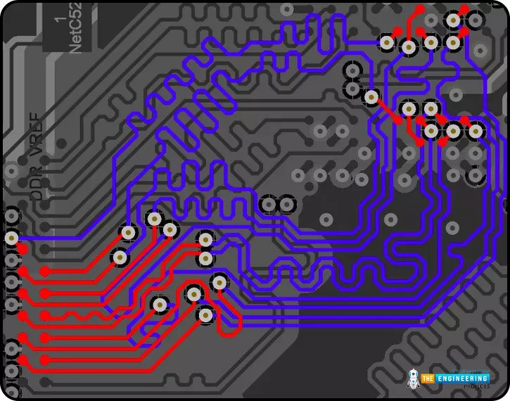
Tuning of the trace length
Here if you are using the high speed interface, you have to do a signal tuning of the length of your traces in order to synchronize your signal propagation. If you miss to do the synchronization, then expect your interface to fail at very high frequencies or even not to work at all. Therefore, the tuning aspects is a very important aspect when it comes to high speed designs.
- In any high speed design, there shall be two types of interferences and that is the parallel and the serial interface.
- The parallel interface will involve the length of the trace tunning only while for the serial interface signals are united into several differential pairs.
- The tunned differential pair
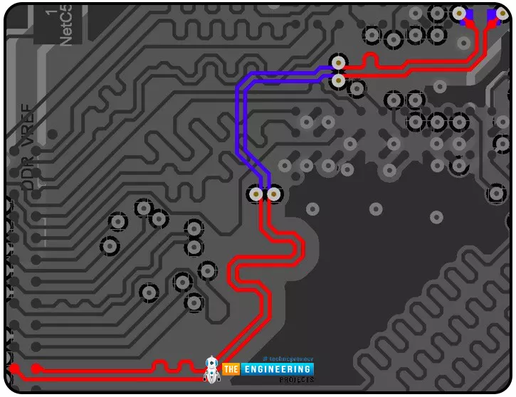
- Below is the tuned length of tracks;
- Tuned parallel interfaces.
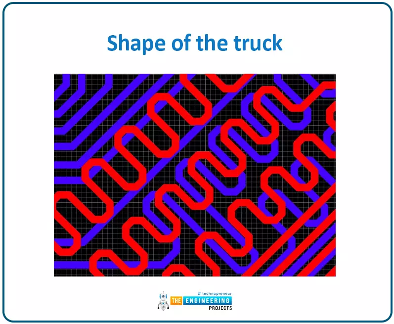
Shape of the truck
It is very rare to meet straight tracks from the source to the receiver on a PCB especially when the high speed design is involved because you have to keep bending the tracks while looking for track locations that will fine tune the trace. In real sense, tracks required smooth, rounded corners without sharp bending and you will need a lot of time to make that possible. What makes since task more time consuming is the fact that you will have to redo this so many times repeatedly until you get the optimized path.
Don’t bent tracks at 90 degrees because the width of the track changes affecting the impedance of the track. It is advised you do the bending at 45 degrees as shown in the figure below;
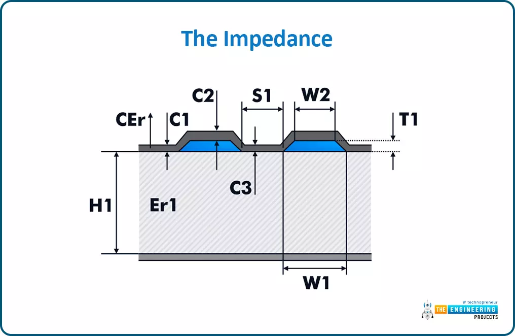
The impedance
Any time you are doing a PCB design, it is very important to make an observation of the single-end point ZO impedances and also as well as the differential impedances Zdiff.
Adherence to the correct impedance is one of the most important rules in the design of the PCB.
Given below are the parameters for the differential impedance calculations;
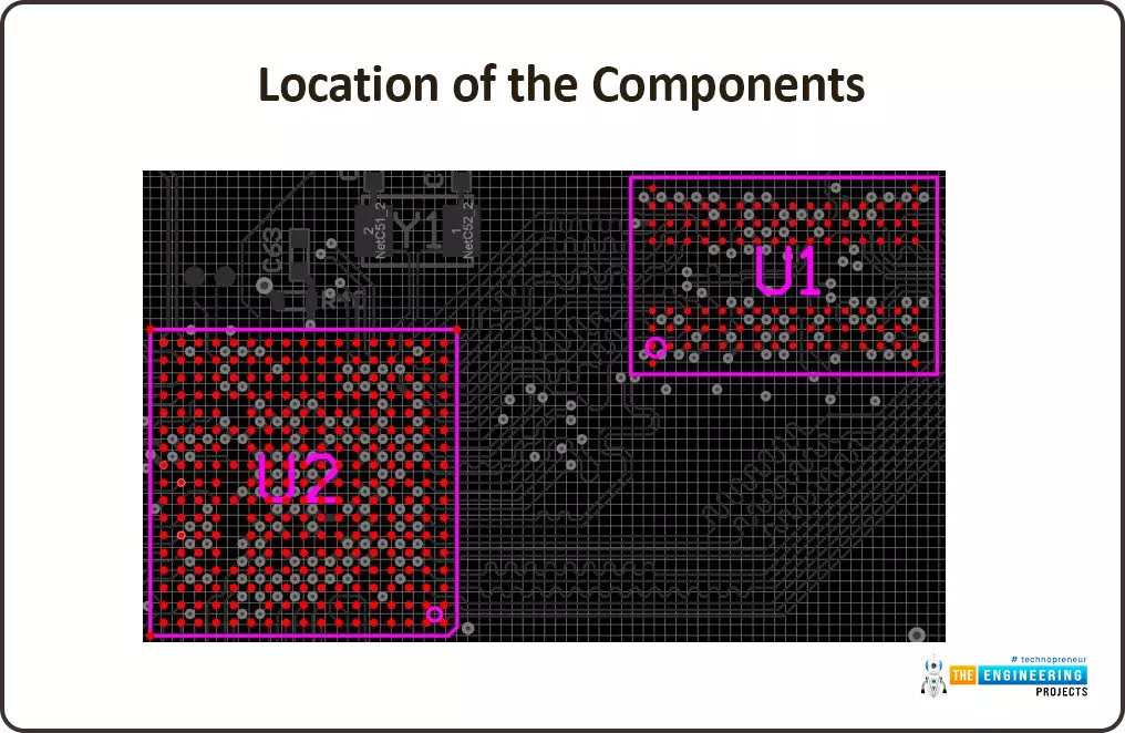
Location of the components
Component placement is one of the most important rules in process of high speed PCB design. Before you begin this process, you have to mark where you are going to place your component.
For example, you can place components according to their functions. If components do same functions or even related purpose, they should always be in the same location to each other.
Analog components should be placed in their locality, with their ground different from others to avoid the EMI.
During placement, remember that the tracks are not long and therefore you should ensure that you leave the space for tuning.
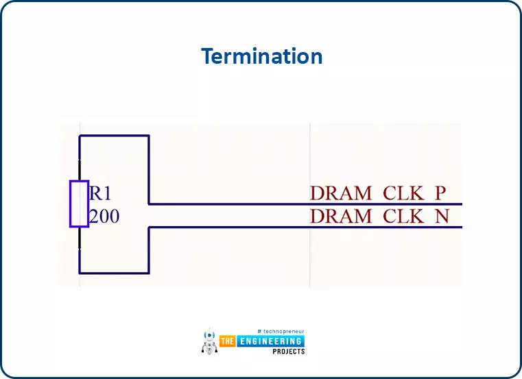
Termination
Most common type of termination is the parallel termination. This is where a resistor is placed in the track between the differential pair and as close to the receiver as possible.
The purpose of termination is for getting rid of the reflected signals in the truck and this leads to the upgrading of the data that is being transferred. When differential pairs are used, the resistor should be equal to the differential impedance or less than the differential impedance.
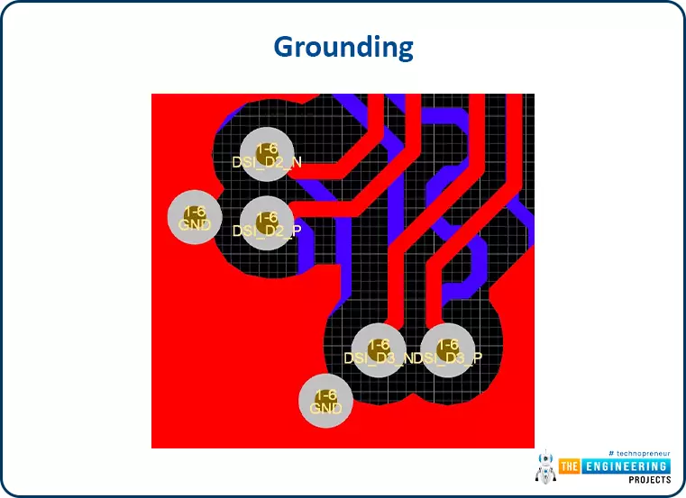
Grounding
In most occasion, it is very impossible to completely trace high speed interfaces in a single layer and this will require introduction of vias in order to move the traces from one layer to another.
Vias are just electroplated holes that allows you to move the tracks from one layer of the board to the other.
It is very important to ensure that you accompany the track via with a ground via. These vias are called stitching vias and they help in maintaining the use of a single reference point in the high speed PCB design.
Tips for high speed PCB design.
Start with a plan
This is a basic thing in PCB design and it is very important to have a plan to avoid so much errors and issues in the design process. So before doing any connections of the symbols or the net list you need a checklist at hand so that you can confirm what to do next to ensure that you have done everything accordingly. The plan will help in;
- Organization of the system
- The power supply
- The signal speed
- Sensitive signals identification.
This are not the only things that you will consider during planning but it is among the first things to do.
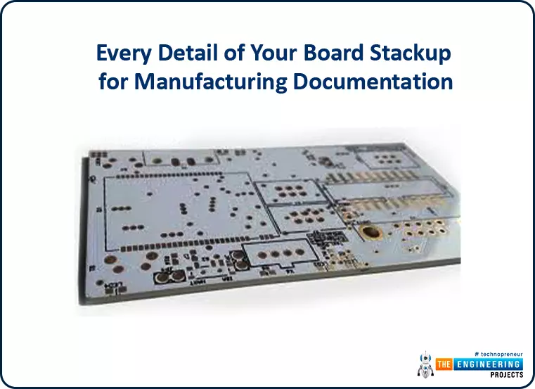
Every detail of your board stackup for manufacturing documentation.
After having the plan, the next thing is to ensure that your layer stackup are documented. This is where you have to contact your manufacturer in order to know which material you will use in the design and also and what type of constraints you should employ in those designs.
Expect to work with the following type of materials;
- FR-4
- Nelco
- Rogers
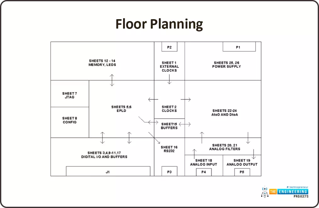
Floor planning
Here you have to organize your board into logical sections. Remember high speed boards are organized into many subcircuits and it is your duty as a designer to determine where each subcircuit should be placed.
This is more so for the case of the analog and digital signals which require that they placed in separate places so that they cannot interfere with each other.
Your physical floor planning should have something like what is below;
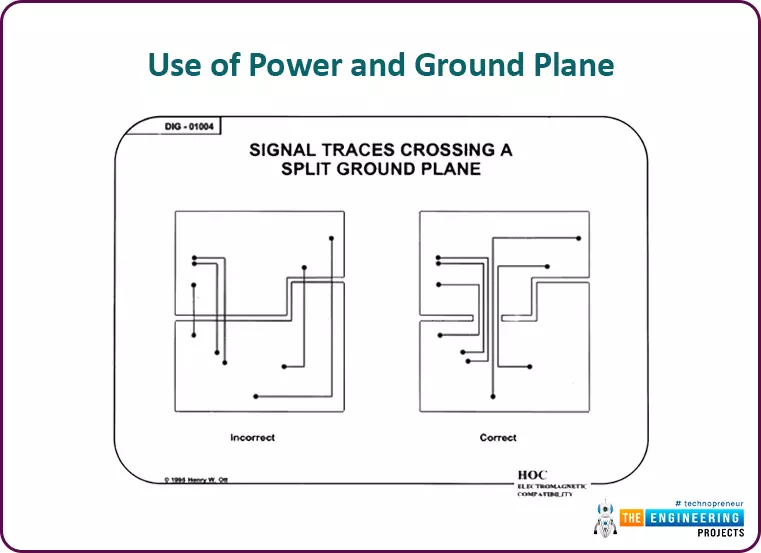
Use of power and ground plane
Now that your plan and stackup is fully laid, it is time to get into important details that you will need in order to start the design.
The size of your land patterns should be kept at minimal.
I the previous design, you might have been using very large pads maybe for easier soldering and inspection. For the high speed design, the space you leave is the key for the success and therefore pads should be 0 to 5% of the size of the components. This drop in space will always help in improving the mechanical strength of the board.
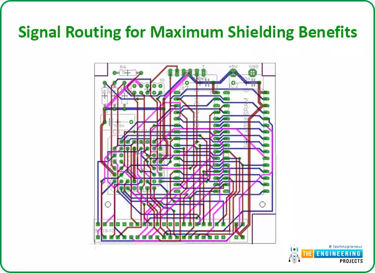
Signal routing for maximum shielding benefits
The high frequency signals will be producing a lot of electromagnetic effects as they travel from the source to the sinking region. And this might lead to two signals having an interference on each other. To avoid this, consider each of the following;
- Minimize parallel signals
- Ensure you maintain us much distance between your signals as possible
- Signals between layers should be routed orthogonally.
Efficient path for current should be provided.
This will involve the use of vias so that to avoid the current path from crisscrossing each other or the ground and to make sure that the signal integrity is maintained.
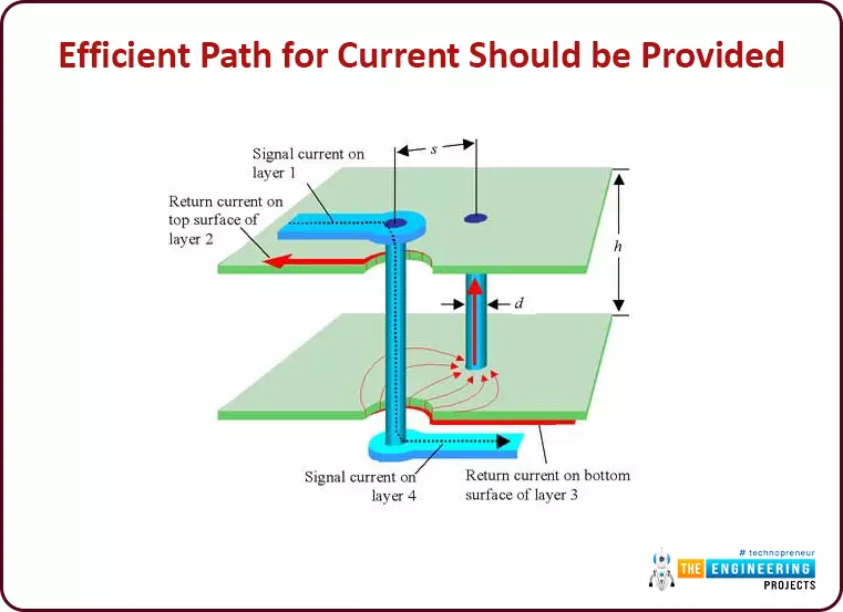
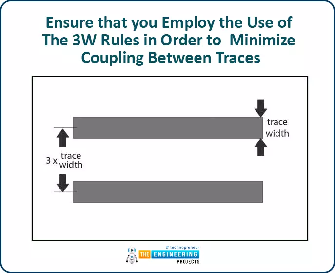
Ensure that you employ the use of the 3W rules in order to minimize coupling between traces.
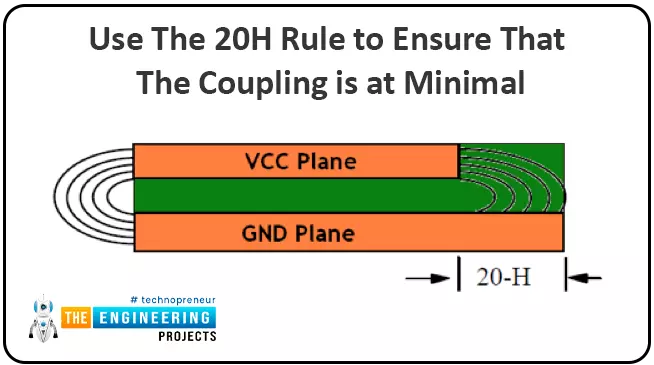
Use the 20H rule to ensure that the coupling is at minimal.