


Junction Field Effect Transistor (JFET) Simulation in Proteus ISIS


Introduction to JFET
We Define the JFET as:"Junction Field Effect transistors or simply JFET is the semiconductor ,Voltage Control, three terminal device that is present in both configurations either N channel or P channel."JFET are named so because the the operation of JFET relies on the Field of the input gate voltage thus they are voltage operated devices. The Input of JFET is called Gate whereas, the output is said to be Drain.
Explanation about JFET
Junction Field Effect Transistors are important Devices in the world of electronics. They look similar to the transistors but are different in their Production.Terminals of JFET:
JFET's have two Ohmic connections at either side of the channels. These channels are called Source and Drain. the Connection of Drain and source is said to be Gate. This is the point where PN Junction is formed. Source and Drain Collectively makes resistive path through which the current Id passes due to the Voltage Vds. The channel is semiconductor due to which current is passed equally well at both sides. But, because of the resistivity of the channel, the voltage becomes less Positive when we move from Drain to Source. Subsequently, the PN junction contains the high reverse bias at Drain as compared to the Source. Thus, the a Depletion Region is formed due to biasing whose width increase with the increase in the Biasing and vise Versa.Configuration of JFET:
We know that Transistors are made by two type of materials i.e, N type and P type. The Terminals are connected by a current path between Drain and Source. these two terminals work as Collector and Emitter, respectively. Hence we observe two Configurations of JFETs:- N-Type.
- P-Type.
Types of JFET:
Base upon their Production, we classify the JFET in two types:- Standard JFET
- Insulated Gate JFET
Conduction of JFET:
JFET are unipolar Devices and their efficiency mainly depends upon the Conduction of holes and electrons in P-Channel and N-channel, respectively.Implementation of JFET in Proteus ISIS
The Junction field effect transistors has very specific characteristics that can easily observed on the graph at a glance. Hence, let's start the simulation for best understanding.Material Required:
- Junction Field Effect Transistor (2N3819)
- DC Power Supply
- Ground Terminal
- Current Probe
- DC Transfer Curve Analysis
Procedure for the characteristics of JFET:
- Fire up your Proteus Software.
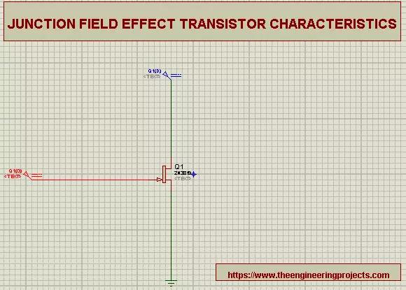
- Pick Up the JFET from the Pick Library through the "P" button.
- Set the JFET on the working area.
- Foster the "DC" from the power Generation mood of the Proteus.
- Fix 1 DC power supply at the Gate Terminal and the other on the Drain Terminal.
- Pick the Ground terminal from "Terminal mode" and fix it with the Source.
- At this stage, the circuit should look like the picture given below:
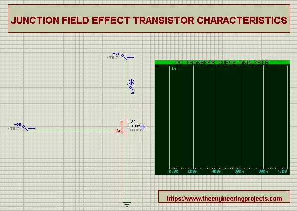
- Place the Current probe taken from the side of the Proteus at the Drain.
- Name the Gate source as "Vgs".
- Name the Drain power supply as "Vds".
- Mark the Current Probe as "Ids".
- Choose "Transfer" from the Graph mode at the left most bar of the Proteus.
- Click on the Working area and make a window of the "DC Transfer Curve Analysis".
- To get the output, we will drag the Id at the graph area.
- At the instance, we have to set the Graph according to our need. Truss, Double click the graph to edit the Properties.
- Set the Values according to diagram:
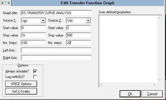
- Simulate the graph through the Play button.
- Maximize the screen through left click at Graph>maximize and Observe the output.
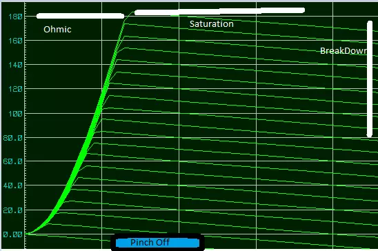
Observations of JFET Characteristics:
- Vgs applied to the Gate Controls the Current flowing between Drain and the Source.
- No current flow through the Gate hence the Source current that is flowing out of the device is equal to the Drain current moving into the device.
Is=Id
- We observe the four types of regions here:
- OHMIC Region: JFET acts like a voltage resistor when voltage VGS =0 because the depletion region at this point is very less.
- Pinch-off region: Resistance is maximum when Vgs is sufficient to cause the JFET to act as an open Circuit. This region is also called Cut-off region.
- Saturation Region: In this Region, the JFET becomes the Good Conductor and be controlled by Vgs. The Vds has very less effect.
- Breakdown Region: We observed that the in this region, the Vds becomes maximum and is controlled.
Advantages of JFET:
- They are replaced by the BJT because they are similar to BJT in characteristics like efficiency , robust, instant operation but are smaller than the equivalent Bipolar Junction Transistors. Thus they are better.
- Due to the size, they have less power consumption and low power dissipation, therefore are ideal to use in ICs and the CMOS range of circuit.
- They have extremely high input Impedance tat can be more than thousands.
×
![]()


