


Introduction to 74HC595


Introduction to 74HC595
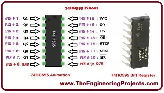
74HC595 is a shift register having and eight bit storage register and an eight bit shift register. The data is written first and then stored into the device. It is high speed CMOS device. The data is usually entered in a serial format. Storage register is used to control the output lines of 74HC595. It has different real life applications e.g. in home appliances, computer peripherals, serial to parallel converter etc.1. 74HC595 Pinout
- It has 16 pins in total out which eight are on left side and the remaining on the right side of the structure.
- The different function is associated with each of the pin.
- Some of the pins acts as an input to this device and receives data serially and transfer to the output pins to observe the received data.
- The pin diagram for 74HC595 is shown in the figure below:
- DS pin acts and receives the serial data.
- All of the lines with prefix Q acts as the output lines.
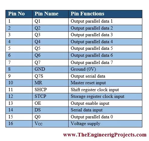
2. 74HC595 Pin Configuration
- In this section if the tutorial Introduction to 74HC595, I will tell you about the functions associated with each of the individual pin of 74HC595.
- All of the associated functions are describes in the table given below.
3. Functioning Diagarm
- The proper functional diagram of the shift register 74HC595 is shown in the figure below.
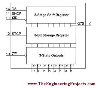
- From the above figure you can see that SHCP, master reset (MR) and the input DS are connected to 8 stage shift register.
- Pin number 12 i.e. STCP is connected to 8 bit storage register.
- The output enable (OE) is connected to 3 state outputs.
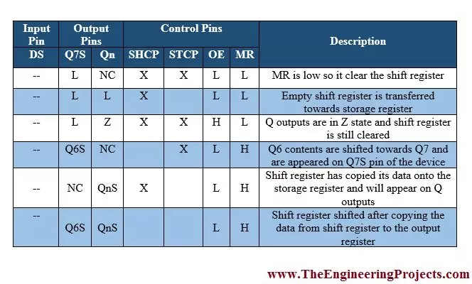
4. 74HC595 Functional Description
- In this section of the tutorial Introduction to 74HC595, I will tell you about the functions of each line of the 8 bit shift register 74HC595.
- Complete description of the functions of 74HC595 is given in the table shown below.
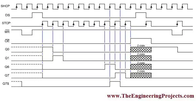
5. 74HC595 Timing Diagram
- The arrow in the upward direction shows the rising edge of the each wave either received or applied.
- The shape of the signals applied and received and their relation with each other is shown in the figure below.
5. 74HC595 Logic Diagram
- The logic diagram for 74HC595 8 bit shift register is shown in the figure below.
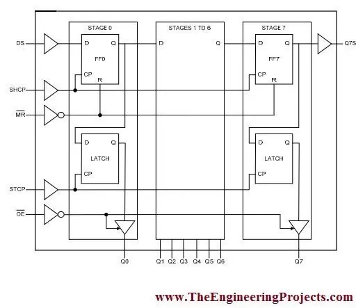
- You can see that there are 8 different stages from 0 to 7 and latches are there in the logic diagram of 74HC595.
- Output enable (OE) and master reset (MR) are connected to latches with an inverted sign usually known as bubble.
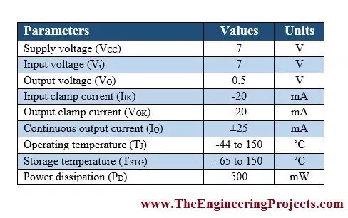
6. 74HC595 Current/Voltage Rating
- The current, power and voltage rating along with their values and system international units are shown in the table given below.
- The values of operating temperature and storage temperature are also shown in the figure below.
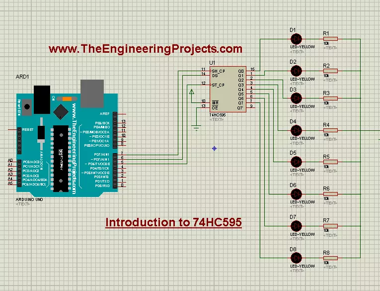
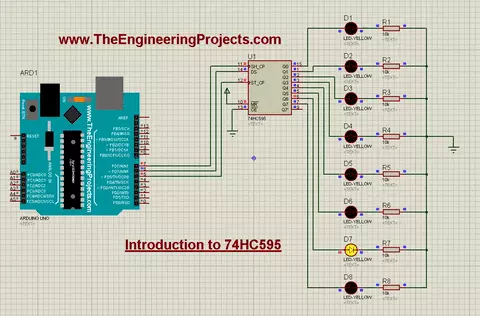
7. 74HC595 Proteus Simulation
- I have a Proteus simulation for continuous control of the different LED's using 74HC595.
- The screenshot of the simulation is shown in the figure below.
- The complete Arduino source code is shown below.
- You need to just upload .hex file of this code into the Arduino of Proteus and run the simulation.
int RCLK = 5;
int SER = 6;
int SRCLK = 7;

#define TotalIC 1
#define TotalICPins TotalIC * 8

boolean Data[TotalICPins];

void setup()
{
  pinMode(SER, OUTPUT);
  pinMode(RCLK, OUTPUT);
  pinMode(SRCLK, OUTPUT);

  ClearBuffer();
}


void loop()
{
   for(int i = TotalICPins - 1; i >=  0; i--)
   {
      Data[i] = HIGH;
      UpdateData();
      delay(300);
      ClearBuffer();
   }

   for(int i = 1;i < TotalICPins - 1;  i++)
   {
      Data[i] = HIGH;
      UpdateData();
      delay(300);
      ClearBuffer();
   }

}
- The running form of the above simulation is shown in the GIF below.
- You can download the complete simulation as well as the complete Arduino source code, here by clicking on the button below.
Proteus Simulation & Arduino Code
- Just download .rar file, extract it and enjoy the complete package having both Arduino source code as well as Proteus simulation.
×
![]()


