Introduction to BF259


Introduction to BF259
- BF259 is a bipolar silicon transistor which is made up of two N doped layer and one P doped layer.
- It is mainly a three terminal device which consists of emitter base and collector.
- P terminal of the transistor acts like a base while other two sides of P layers act as emitter and collector respectively.
- Small current at the base is used to control a large amount of current at the collector and emitter side.
- The power it can dissipate is 1 W, while transition frequency is about 75 MHZ.
- DC collector current is 100mA.
- Maximum power dissipation across collector is 0.5 W.
- BF259 is also considered as a current operated device.
- Maximum collector base voltage is 300 V and is denoted by Vcb.
- Maximum collector emitter voltage is 300 V and is denoted by Vce.
- It comes with lots of major applications but mainly it is used for switching and amplification purpose.
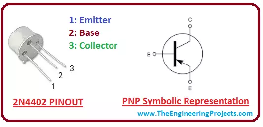
1. BF259 Pinout
BF259 NPN silicon transistor consists of three terminals. 1: Emitter 2: Base 3: Collector Actual pinout of this NPN transistor is given in the figure below
- The base current is used to control the large amount of current on the collector and emitter side.
- The way the base current impact the emitter and collector current is used for the amplification applications.
- This bipolar transistor will turn ON when current flows from emitter and collector.
2. Mechanical Outline of BF259
The mechanical outline of bipolar silicon transistor BF259 is shown in the figure below:
- All the dimension are given in mm.
- You must take these dimension into consideration before you plan to make a circuit so these dimension properly fit in the circuit.
3. Circuit Diagram of BF259
The circuit symbol of BF259 is shown in the figure below:
- This NPN silicon transistor comes with a positive base side and negative emitter side.
- Emitter current is the sum of base and collector current.
- Small amount of current at the base side is used to handle the large amount of current at the emitter and collector side.
- Main difference between NPN and PNP transistor is, Current will sink into the base side in case of PNP transistor while current from the base side will source to the transistor in case of NPN transistor.
- Transistor current can be found by dividing the collector current to the base current. It is also called beta current and is denoted by ß. Beta has no units as it is a ratio between two currents.
- Value of beta is used for the amplification purpose. Beta value ranges between 20 to 1000, however, its standard value is 200.
- The ratio between collector current to the emitter current is called current gain of the transistor and is denoted by alpha a.
- The value of alpha ranges between 0.95 to 0.99, however, in most of the cases it is considered as 1.
4. Absolute Maximum Rating BF259
The maximum absolute rating of BF259 is shown in the figure below.
- Units of current and voltage are mA and V receptively.
- These rating are important for many engineering projects.
5. Applications
- BF259 is also called high voltage video amplifier and is mostly used for high voltage video output.
- It is also used for the audio output stages.
- These transistors are the main drivers for horizontal deflection circuits.
×
![]()