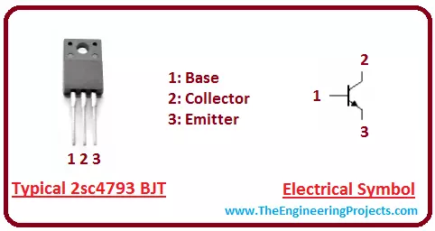
Introduction to 2n1711


Introduction to 2n1711
- 2n1711 is an NPN bipolar junction transistor which is mainly used for switching and amplification applications.
- It consists of three terminals called emitter base collector and comes in TO-39 case style.
- It is a current controlled device where small current at the base side is used to control large current at the emitter and collector side.
- 2n1711 is a bipolar device where conduction is carried out by movement of both charge carriers holes and electrons.
- When we apply positive voltage at the base side, it gets biased and allows to control large current at the emitter and collector side.
- Base is actually acts like a handle which actually controls the flow of electrons emitted by emitter.
- These electron are then collected by collector. So base is actually controlling the conduction from emitter to collector terminals.
- In this NPN transistor, emitter is heavily doped while base side is lightly doped.
- Base side is positive with respect to emitter and P layer of this transistor lies between the two N-doped layers.
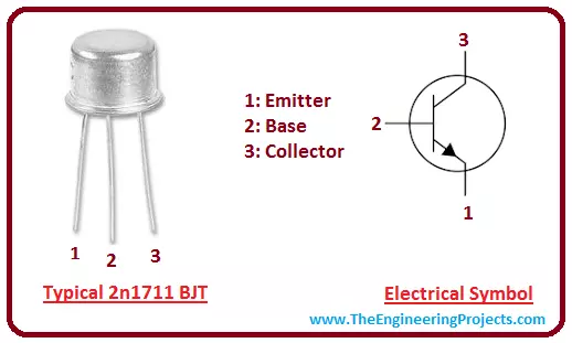
2n1711 Pinout
2n1711 mainly consists of three terminals which are described below.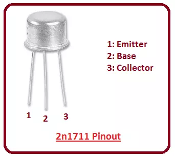
- Small current at the base side is used to control the large current at the emitter and collector side.
- This process of controlling large current with the help of small current is used for amplification purpose.
- This transistor is mainly composed of silicon.
Circuit Diagram of 2n1711
Circuit symbol of 2n1711 is shown in the figure below.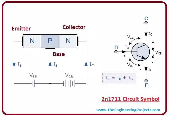
- This NPN transistor can be configured into three main configuration i.e common base configuration, common emitter configuration and common collector configuration.
- Common emitter configuration is widely used for amplification purpose because it features the required voltage and power gain for amplification purpose.
- This configuration allows the input to increase by 20dB which is nearly 100 times more than input signal.
- It is important to note that collector voltage is higher than the base voltage.
- Current at the emitter side is the combination of both base current and collector current.
- Main difference between emitter and collector is their size and doping concentration. Collector is lightly doped while emitter is highly doped.
- In this transistor, base current is always the smallest current while emitter current is always the largest current.
- Forward current gain of the transistor is represented by beta ß. It is actually an amplification factor, the value at which current is being amplified. It is the ratio between collector current to the base current. As it is a ratio between two currents so it features no unit.
Absolute Maximum Ratings
Absolute maximum rating of 2n1711 is shown in the figure given below.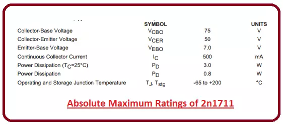
- These are the stress ratings of 2n1711. If values are exceeded from given values, it can harm the device at large.
- Collect base voltage is 75 V while collector emitter voltage is 50 V
- Maximum power it can dissipate is 3 W.
Mechanical Outline of 2n1711
Mechanical outline of 2n1711 is shown in the figure below.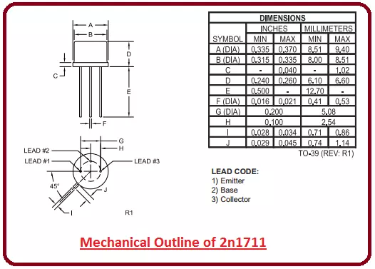
- All dimensions are in mm.
- You must take these dimension into consideration before you intend to make a circuit so these dimensions can properly fit into the circuits.
Applications
- 2n1711 is mainly used for amplification purpose.
- In most of the circuits it is also used as a simple switch. When base is biased with the help of voltage, it allows the current to flow from emitter to collector. And in this state transistor remains in ON mode and acts as an ON switch. When there is no bias involved at the base side, the switch will be OFF.
×
![]()