Introduction to 2n4403

Introduction to 2n4403
- 2n4403 is a PNP bipolar junction transistor where conduction is carried out by the movement of holes and electrons but majority charge carriers will be holes.
- It consists of three terminals named as emitter base collector. N layer represents the base of the transistor while other two layers represent emitter and collector respectively.
- It works similar to NPN transistor where small amount of current at the base side is used to control the large current at the emitter and collector side.
- As it is a PNP transistor so base terminal will be negative with respect to emitter.
- Most of the transistors behave like a switch because when we apply small voltage at the base side, it is used to control the large current at the emitter and collector side and switch will be considered ON.
- When there is no bias at the base side the switch is considered OFF.
- PNP transistors also known as current controlled device because small current at the base side is used to control the large current at the emitter and collector side.
2n4403 Pinout
2n4403 is a bipolar junction transistor which consists of three terminals.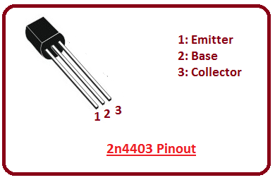
- The small current that leaves the base will be amplified at the collector output.
- This PNP transistor will only conduct if base is negative with respect to emitter terminal.
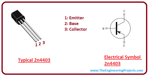
2n4403 Circuit Symbol
Circuit symbol of 2n4403 is shown in the figure below.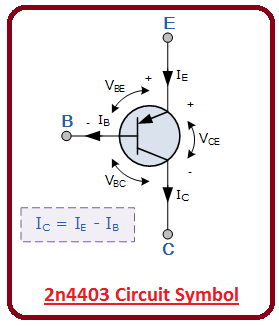
- PNP transistor can be considered normally OFF, but negative voltage at the base side and small out put current can turn it ON and helps in flowing large emitter-collector current.
- PNP will only conduct when voltage at the collector side Vc is much smaller than voltage at the emitter side Ve.
- Current at the emitter side is the sum of current at the base and collector side.
Absolute Maximum Ratings of 2n4403
Absolute maximum ratings of 2n4403 is shown in the figure below.
- It is important to note that if stresses are exceeded from absolute maximum ratings, they can damage the device.
- Similarly if stresses are applied for extended period of time above the normal operating condition, they can effect the device reliability.
Transistor as a Matched Switch
- In most of the cases PNP transistors widely replace NPN transistors and they can also be used as a switch.
- You may come across a question what do we use PNP transistors while NPN can be widely used for switching and amplification purpose. However, when we combine these two different types of transistors, they come with a lots of advantages.
- Class-B amplifiers are incorporated with two pairs of PNP and NPN transistors, where both transistors are used to control the direction of current flowing in both directions at any time.
- Transistors are termed as “Complementary Transistors” which use both NPN and PNP transistor of identical characteristics.
- Both transistors, in Class B-amplifiers, work in a similar way i.e. PNP transistor conducts for the negative half cycle of the transistor while NPN transistors conducts for the positive half cycle. This results in flowing the power at the load out put in both directions. PNP transistors will switch on when it sinks current to its base side and it will switch off when current at the base side stops to flow.
Difference between PNP and NPN transistors
- Both NPN and PNP transistor features same characteristics with some exceptions.
- In case of PNP all the voltage polarities and current directions will be reversed as compared to NPN transistors and majority charge carriers will be holes in case of PNP transistors.
- Also PNP transistor will sink current at the base side while in case of NPN transistor it sources current through its base.
- The base gets biased with the addition of negative voltage which then controls the large amount of current at the emitter and collector side.
- Some professionals prefer NPN transistor over PNP transistors because conduction due to mobility of electrons is considered better than the mobility of holes.
Applications
- PNP can also be used as voltage and power amplification purpose.
- When NPN transistors are incorporated with PNP transistors, they construct a perfect bond through which current flows alternately from both sides of NPN and PNP transistors.
×
![]()


