Introduction to 1n5819

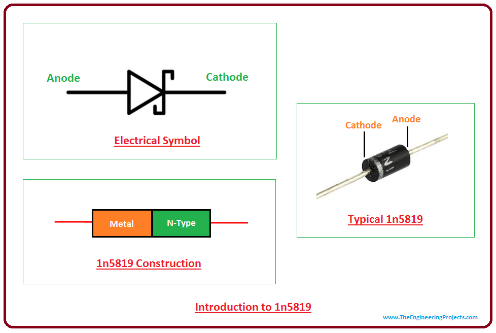
Introduction to 1n5819
- 1n5819 is a metal to silicon power diode that applies Schottky Barrier Principle. It is also referred as Schottky Rectifier(named after Scientist Walter H. Schottky), surface barrier diode, hot electron diode or hot carrier diode.
- This diode is mainly used as a rectifier in many devices including high frequency low voltage inverters, polarity protection diodes, free wheeling diodes and radio frequency applications.
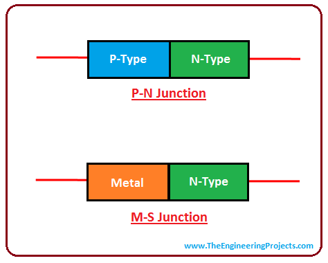
- It is little bit different than normal PN junction diode where metal like platinum or aluminium are used in place of P-Type semiconductor.
- In Schottky diode, semiconductor and metal joined together, forming a metal-semiconductor junction where semiconductor side acts as an cathode and metal side acts as a anode.
- When metal-semiconductor junction formed between metal and semiconductor, they result in depletion layer also referred as Schottky barrier.
- Schottky comes with low stored charge and exhibits low power loss and high efficiency mechanical characteristics.

- It is manufactured in such a way that all external surfaces are corrosion resistant and terminals are easily solderable where current flows in one direction only and it stops the current flowing in other direction.
- Maximum temperature it can withstand for soldering purpose is 260 °C.
- Guard ring die construction gives it transient protection and high surge capability.
- The power drop occurred in this diode is lower than PN junction diodes.
- The Schottky diode is a semiconductor diode that comes with fast switching applications and it pertains to less unwanted noise as compared to PN junction diode which makes it an ideal choice for most of the switching applications.
- When voltage is applied across the diode terminals, current starts to flow which results is small voltage drop across the terminals.
- The voltage drop in this diode lies around 0.15 to 0.45 which is very low as compared to regular diode where voltage drop lies between around 0.6 to 1.7 V.
- The lower voltage drop results in higher efficiency and higher switching speed.
- The voltage drop is actually referred as a voltage required to turn on the diode.
- The voltage required to turn on the germanium is same as Schottky diode, but germanium diodes are not used in most of the applications because they feature very less switching speed as compared to germanium diode.
How Schottky Diode 1n5819 Works
- Working of Schottky diode is slightly different than normal PN junction diode where P-Type semiconductor is replaced by metal.
- When metal and semiconductor are joined together, they shape a metal-semiconductor junction which allows the flow of electron from higher energy level to lower energy level.
- As the electrons available in N-Type semiconductor exhibit more energy and start flowing from semiconductor to the metal region.
- We know when atom loses an electron, it results in positive ion and when atom gains electrons it results in negative ion.
- Similarly, when N-Type semiconductor loses electron, it clothes positive charge on it and the electrons that go to the metal allow it to cloth negative charge on it.
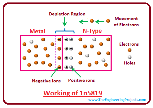
- The positive and negative charges appearing on the metal and semiconductor region are nothing but the depletion region.
- The electronic width available in the n-type semiconductor is much larger than the electronic width that allows the electron to move from semiconductor to the metal.
- Basically built-in-voltage houses inside the semiconductor that can be seen by the conduction bands when electrons try to move to the metal region.
- In order to move electrons from semiconductor to the metal region, the positional energy of the electrons must be greater than the built-in-voltage.
- We are referring unbiased Schottky diode where only small number of electrons pass from semiconductor to metal region because built-in-voltage creates a barrier which refrains the large movement of electrons from semiconductor to the metal region.
Absolute Maximum Ratings of 1n5819
Following figure shows the absolute maximum ratings of 1n5819.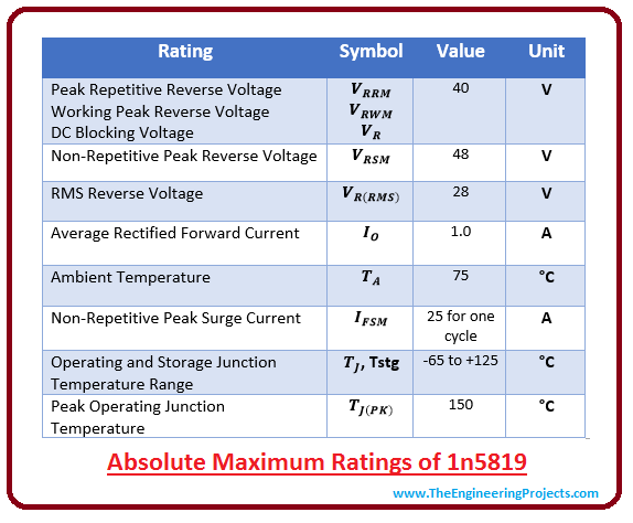
- It is important to note that these are the stress ratings, which if exceed from absolute maximum ratings, can damage the device severely.
- Similarly, if stresses are applied for extended period of time, they can effect the reliability of the device.
Comparison between Schottky Diode and PN junction Diode
- There are number of differences between Schottky diode and PN junction diode. The Schottky diode is a uni-polar device because conduction is carried out by the movement of electrons only. Conduction through holes is very negligible as compared to conduction through electrons.
- PN junction diode is a bipolar device where conduction is carried by the movement of both charge carriers i.e. electrons and holes.
- In Schottky diode, the reverse breakdown voltage and depletion region is very small or negligible as compared to silicon PN junction diode.
- Similarly, the voltage drop across Schottky is very low as compared to PN junction diode which makes it suitable for many switching applications.
Applications
Schottky diodes come with a number of applications including- General purpose rectifier
- Radio frequency applications
- Detect signals and power supplies
- Logic Circuits
- Polarity protection diodes
- Free wheeling diodes
×
![]()


