Today, I am going to add one more article in this series and discuss the details on the Introduction to Diode. It is an electronic device that allows the flow of current in one direction only.
Hi Guys! Hope you are doing great. Today, we will have a look at an electronic component named Diode. We will discuss Diode working, Symbol, Applications and characteristics in detail.
A diode is an electronic component, that allows the flow of current in one direction only. It exhibits low resistance in one direction and very high resistance in the opposite direction. Whoever has been a science student, knows about diodes. Although it seems to be a tiny component of a circuit, apparently it is true but it has a lot of complexities or you can say, it's a storm in a teacup.
Diodes are normally used in rectifiers, where they convert AC signals to DC signals. They come with a wide range of applications including power conversion, radio modulation, logic gates, temperature measurements and current steering. I'll try to cover everything related to diodes so let's get started:
Diode Definition
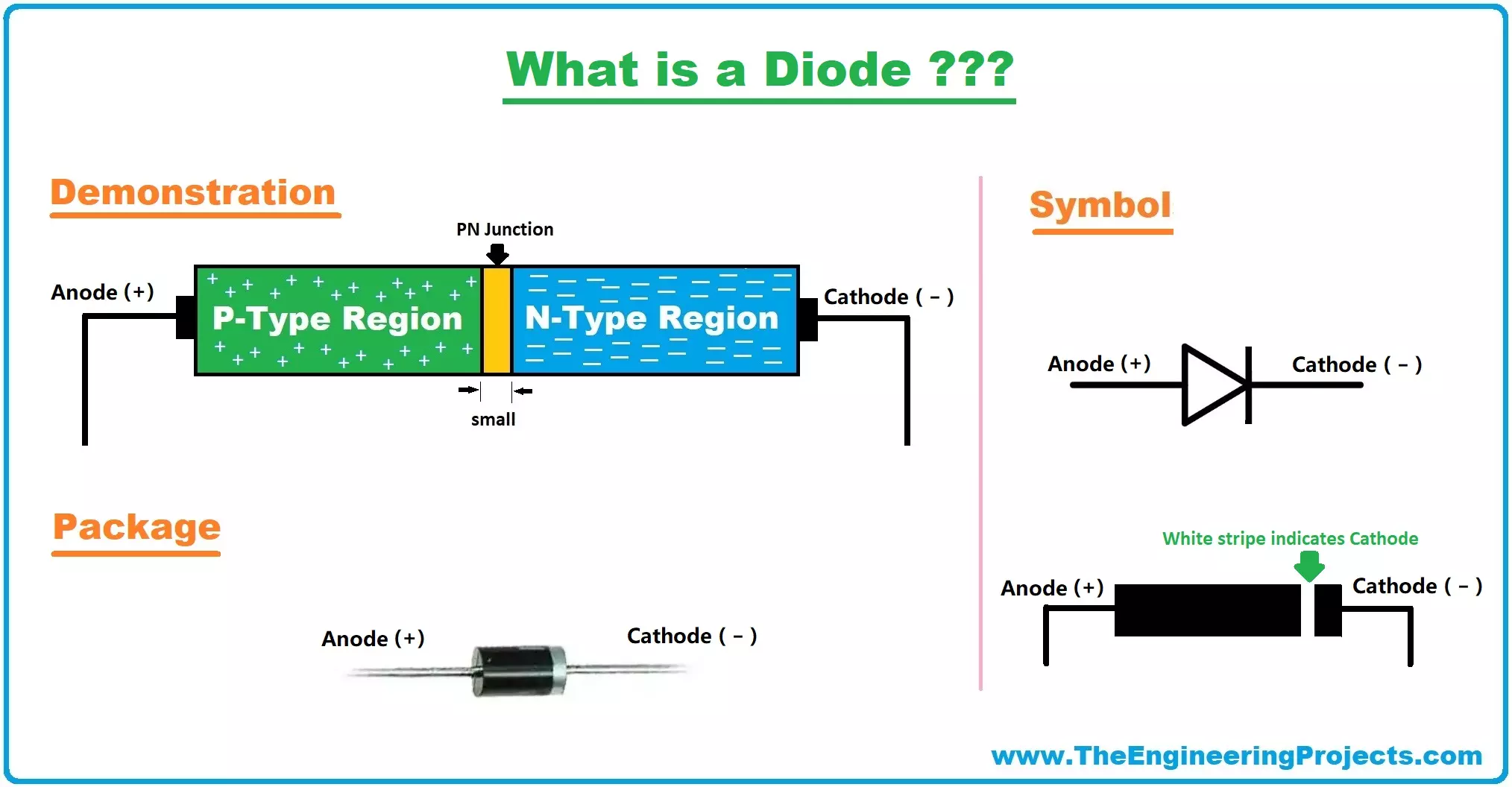
A diode is a 2-terminal, basic discreet electronic component, made up of semiconductor material, which allows a unidirectional flow of current through it, i.e it only conducts current in one direction.
A diode is analogous to a uni-directional water flow valve, which allows the water to flow in one direction but restricts it to flow backward.
Diode consists of two terminals, named:
Anode (+).
Cathode (-).
These terminals are connected to two doping regions:
P-Type region.
N-Type region.
The P-Type region consists of positively charged ions called Holes, while the N-Type region consists of negatively charged electrons. We will discuss its construction in detail later.
In a diode, current flows from Anode to Cathode(diode acts as a closed switch), but if the current flows in the opposite direction(i.e. from Cathode to Anode), the diode will block it, so we can say, the diode is acting as an open switch.
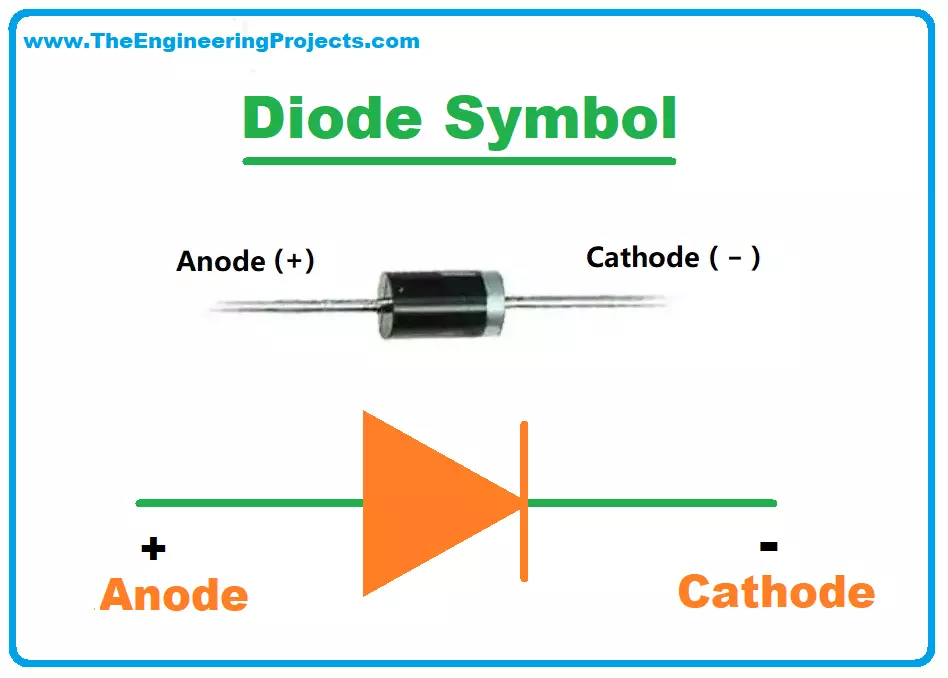
Diode Symbol
The diode symbol and its real package are shown in the below figure:
The arrowhead in a diode symbol represents the direction of the current flow i.e. current can flow from anode to cathode.
Construction of Diode
Now let's have a look at the construction of a diode:
A diode is normally made up of a semiconductor material i.e. silicon, germanium, gallium arsenide etc.
Two crystals of the same semiconductor material(normally silicon) are doped with different types of impurities, one crystal with pentavalent impurity, while the second one with trivalent, to create two types of semiconductor materials named:
P-Type Semiconductor: Majority Charge Carriers are Holes(+).
N-Type Semiconductor: Majority Charge Carriers are Electrons(-).
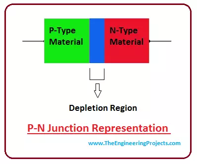
When these two semiconductors are joined/merged together, the free electrons from the N-Type start to move towards the P-Type region, while the Holes start moving towards the N-Type region.
At the border of these two regions, electrons get combined with Holes and neutralized.
These neutralized atoms create a layer at the border(of N-Type & P-Type regions) and stop the flow of electrons & Holes. This newly created third layer/region is called the depletion region.
The depletion region is very small in size and acts as a barrier for the flow of charge carriers(i.e. electrons & Holes) from the N-type to P-type region.
Below diagram will give you a better idea of Diode construction:
As you can see in the above figure, we have 3 regions in a final diode, named:
N-Type Region: Majority Charge Carriers are Electrons(-).
P-Type Region: Majority Charge Carriers are Holes(+).
Depletion Region: No Charge(Neutral)
Two electrically conductive electrodes/probes are connected to these two Regions and are called:
Cathode: Connected to N-Type Region.
Anode: Connected to P-Type Region.
You must have understood by now, how diodes are constructed? Now, let's have a look at How diode works?
Diode Working
As we discussed in the above section, when two semiconductor materials are merged together, a momentary flow of charge carriers occurs, which results in the creation of a depletion region. This state of the diode is normally termed as Zero Biasing State, as there's no power applied at any terminal.
In operational mode, the diode has two other biasing states, named as:
Forward biased.
Reverse biased.
Diode as Forward Biased
The PN Junction created at the center of two regions is very small but it's powerful enough to stop the free electrons from passing through it.
So, if we could provide some external power to these electrons, they can break this barrier and can make their entry into the P-Type region.
This external power required to overcome the depletion region is normally termed as a Forward Threshold Voltage of diode.
This threshold voltage value depends on the semiconductor material used in the diode construction i.e. for silicon it's +0.7V and for Germanium, it's +0.3V.
So, for a normal diode, if we provide an external power of +0.7V, the electrons will overcome the depletion region and in simple words, the current will start flowing through the diode.
As you can see in the below figure, the positive terminal of the battery is connected with the anode of the diode and as we will provide a voltage greater than its threshold voltage, the diode will start conducting and is said to be acting as forward biased.
In forward biasing conditions, an ideal diode has zero resistance, but as I told you earlier, an ideal condition does not exist.
Diode as Reverse Biased
If the polarity of the applied power is reversed i.e. positive terminal of the battery gets connected with the cathode(-), while the negative terminal gets connected with the anode(+), the depletion region will start to increase.
In this state, the diode won't allow the current to flow through it and is said to be acting as reverse biased.
In a reverse Biased state, the diode acts as an open switch.
The PN junction in reverse biasing offers a very high resistance due to the thickness of the depletion region.
A diode in ideal condition when reverse biased has infinite resistance.
History of Diode
Introduced in 1906, the first semiconductor diode was named as Cat's Whisker Diode that was fabricated using mineral crystals.
Mostly, diodes are designed using silicon because it can handle high temperature, however, germanium is also used when low voltage drop is required.
When there is no applied voltage across the diode terminals, the diode will not conduct and very thin depletion region exists with no charge carriers around the pn junction of the diode.
The diode will only conduct when applied voltage at the forward biased condition is greater than the diode built-in potential and it allows the flow of electrons from the cathode to the anode.
Don't get confused with the arrow sign of the diode pointing from the anode to the cathode. It shows the conventional current flowing from anode to cathode. Conduction will be carried out from cathode to anode when a certain voltage above built-in potential is applied.
A diode will stop conducting when the applied voltage is reverse biased and allows the depletion region to expand, blocking the flow of current. However, when a reverse biased voltage is too large, it allows the small current to flow which is called leakage current. It is too small that most of the time it is ignored while considering the current ratings.
Similarly, when the reverse biased voltage is too large, it allows the depletion region to expand too much till it collapses, reaching a condition called breakdown, which appears to be very harmful for the quality and operation of the device.
When we check the value of resistance by multimeter, it shows the low value at one terminal and high value at other terminal which indicates diode is working. It doesn't indicate the actual value of the resistance, instead, it shows the voltage drop across the pn junction.
For silicon diodes, the forward voltage drop is 0.7 V, which is the voltage required to overcome built-in voltage in order to start the flow of current from cathode to the anode. Similarly, forward voltage drop for germanium is 0.3 voltage which makes it an ideal choice for the applications where low voltage drop is required.
The voltage drop is highly dependent on the current flowing through the diode, however, it remains constant over a wide range of currents.
Junction Diodes
Diodes are divided into two types based on the formation of the junction between the terminals.
p-n junction Diode
A pn junction diode is made from semiconductors like silicon or germanium where an N-type region is created with the help of negative charge carriers called n-type semiconductor while the P-type region is created with the addition of positive charge carriers called p-type semiconductors.
Initially, there is no flow of current between two regions until they are joined together, resulting in a formation of pn junction where movement of electrons starts from N-type semiconductor to P-type semiconductor.
There exists a region around pn junction where there are no charge carriers called depletion region. When depletion is very thin, indicates a conduction from N-type region to P-type region. When deletion region is very large, indicates no or little flow of current between two regions.
The diode action takes place around the pn junction. When forward voltage potential more than built-in potential is applied between the diode terminals, it allows the flow of electrons from N-type region to P-type region, while blocking the flow of electrons in reverse order.
Foward biased mode means the flow of electrons from N type to P type region. Reverse biased mode means no flow of electrons, blocking the current in other direction.
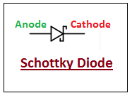
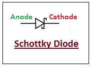
Schottky Diode
Schottky diode is another type of junction diode where the junction is formed using metal-semiconductor instead of using p-n junction. It is an ideal choice for the applications where high switching speed is required.
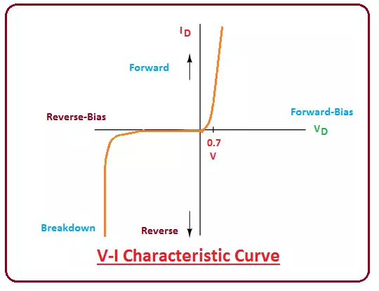
Current-Voltage Characteristics
The voltage in V-I curve shows the voltage applied across the diode terminals and current shows the corresponding current obtained as the result of the applied voltage.
Based on needs and requirements, the V-I characteristics of the diode can be customized using the suitable semiconductor material and doping concentration of impurities during the manufacturing of the device.
The depletion region housed between the pn junction shows how the movement of electrons between the two N-type and P-type regions takes place.
When pn junction is formed, the electrons from N-type region transfers to the P-type region, where they join the holes present in the P-type region.
When electron combines the hole, the resulting pair disappears and the region around pn junction gets depleted with no charge carriers present. Resulting depletion region around the pn junction acts as an insulator.
It is important to note, the width of depletion region cannot exceed without limit. When an electron-hole pair is created, it results in the formation of positively charged ion in the N-type region and negatively charged acceptor ion in the P-type region.
As the formation of electron-hole pair proceeds, it results in the creation of built-in potential where increasing electric field developed around the depletion region, stops the further formation of an electron-hole pair.
Foward Biased Mode
When the external voltage applied between the diode terminals comes with opposite polarity as the built-in potential, it starts the current flow where depletion region acts as a conductor. In this case, the depletion region formed around the pn junction will be very thin.
The built-in potential is different for different diodes i.e. 0.7 for silicon and 0.3 for germanium.
If the external voltage of opposite polarity with more than 0.7 V is applied between the diode terminals in case of a silicon diode, it allows the current to flow from anode to cathode. The diode is considered as "turned on" in this case.
The voltage above which diode starts conducting through depletion region around the pn junction is called forward threshold voltage which is different than the built-in voltage.
Reverse Biased Mode
When the external voltage applied between the diode terminals comes with the same polarity as built-in potential, it allows the depletion region to expand and stops the flow of current where depletion region acts as an insulator.
Types of Diodes
There are many types of diodes available in the market which are mainly used for the customization of voltage or current. Most of the pn junction diodes are made from silicon and germanium. Before the inception of these power diodes, selenium was used to manufacture the diodes.
Selenium diodes come with low efficiency as compared to silicon diodes, because high forward voltage around 1.4 or 1.7 V is required to start conducting around the pn junction, resulting in the need of much larger heat sink. Following are the most commonly used diodes in the electronic devices.
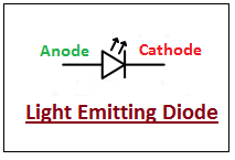
LED Diodes
These diodes are made from the crystalline substance that emits light in different colors like red blue green or orange, depending on the crystalline material used in the diode.
These diodes emit incoherent, narrow-spectrum light, capable of producing wavelengths in the wide range.
Most of the LED diodes are low-efficiency diodes, which make them an ideal choice for the signal applications. LED diodes are also used in the formation of opto-isolator.
Avalanche Diodes
These diodes are very identical to Zener diodes, where they start conducting in the reverse direction when reverse bias voltage becomes greater than break down voltage. These diodes come with an ability to break down at a certain voltage, without destroying them completely.
Both Zener and Avalanche diodes are quite similar with respect to their mode of operation with one practical difference i.e. both didoes exhibit temperature coefficient with opposite polarities.
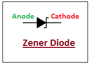
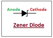
Zener Diodes
Zener diodes, also termed as reverse breakdown diodes, are the diodes that conduct in reverse bias condition.
Zener breakdown effect occurs at a very specific voltage, making them suitable for use as a precision reference voltage.
In reference circuits, temperature coefficient balancing can be achieved by using a combination of zener diodes and switching diodes.
Both avalanche and zener diodes fall under the category of breakdown diodes and electrically they response quite similar with one exception i.e. zener diodes operate with a breakdown voltage below 5 V, while avalanche diodes operate with a breakdown voltage above 5 V.
Crystal Diodes
Crystal diode, also known as Cat's Whisker diode, is point contact diode which is not easily available in the market. This diode comes with a thin metal, known as an anode, and semiconductor crystal, known as a cathode.
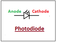
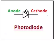
Photodiodes
Photodiodes are composed of semiconductor materials that are light sensitive, making them an ideal choice for solar cells and optical communications.
These diodes are mostly available in single diode package, however, single dimensional or double dimensional array combination is also widely available.
Applications
Diodes allow the current to flow in one direction which makes them suitable for most of the applications where current controlling is prerequisite. Following are the major applications of the diodes.
ONE. Logic gates are designed using diodes with other electronic components.
TWO. Diodes are also used as a waveform clipper, where they clip the negative or positive peak of the signal in order to attain specific voltage.
THREE. Didoes are helpful for temperature measuring because the forward voltage drop across them is very sensitive to temperature. Most of the diodes come with negative temperature coefficient which remains constant above 20 Kelvin.
FOUR. Diodes are widely used for the demodulation of amplitude signal. The amplitude of AM signal is directly proportional to the original audio signal and comes with positive and negative peaks of the carrier wave. The diode is used to rectify the AM radio signal, resulting in only positive peaks of the carrier wave. A filter is applied in order to extract the audio signal from radio carrier wave, which then produces sound waves when applied to the amplifier.
FIVE. Rectifiers are made from diodes which widely replace the commutator for converting AC signal to DC signal.
SIX. Some electronic circuits are very sensitive and show high spikes in the voltage during the execution of the project. These diodes are used to prevent the circuits from high voltages spikes which appear to be very damaging, if not controlled properly, in the early stages.
That's all for today. I hope you have found this article useful. If you're unsure or have any question, you can approach me in the comment section below. I'd love to help you according to best of my expertise in any way I can. Feel free to keep us updated with your suggestions, they help us to provide you quality work that resonates with your needs and demands. Thanks for reading the article.
syedzainnasir
I am Syed Zain Nasir, the founder of The Engineering Projects (TEP). I am a
programmer since 2009 before that I just search things, make small projects and now I am sharing my
knowledge through this platform. I also work as a freelancer and did many projects related to
programming and electrical circuitry. My Google Profile+Follow
Get Connected
jerin
Says:
Thanks for this Informative post.
Reply
100
1
jared
Says:
Iam very thankful for the notes and i have enjoy and understand reading them.
Iam a student at college level persuing diploma in electrical and electronics engineering first year . What can l do to perform best in that cause.
I need your response thank you in advance.
Reply
100
2
djamila
Says:
I thank you
I am very happy with you
Reply