

Hey Guys! I hope you all are doing great. In the previous tutorial, we studied the basics of Semiconductors, where we briefly discussed the PN Junction. Today, we are going to have a detailed overview of PN Junction.
But before getting into the details of PN Junction, we need to first recall a few concepts from the previous lecture:
Semiconductor Basics
As we know, the conductive power of a semiconductor material lies between a conductor and an insulator. So, it can act as a pure conductor as well as a pure insulator, depending on the applied conditions.
Semiconductors are divided into two types:
- Intrinsic Semiconductor.
- Extrinsic Semiconductor.
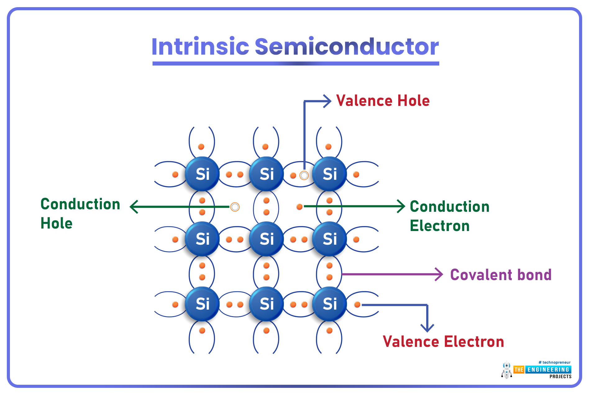
Intrinsic Semiconductor
- A semiconductor in its pure form is called an Intrinsic semiconductor.
- In this state, the outermost valance shell of the semiconductor has an equal number of electrons and holes(which is 4).
- These four valance electrons in the outermost shell of an Intrinsic semiconductor remain bound to their positions and thus no conduction is allowed.
- So, an Intrinsic Semiconductor acts as a pure insulator.
- The elemental Silicon(Si) or Germanium(Ge) in its pure form is an intrinsic semiconductor.
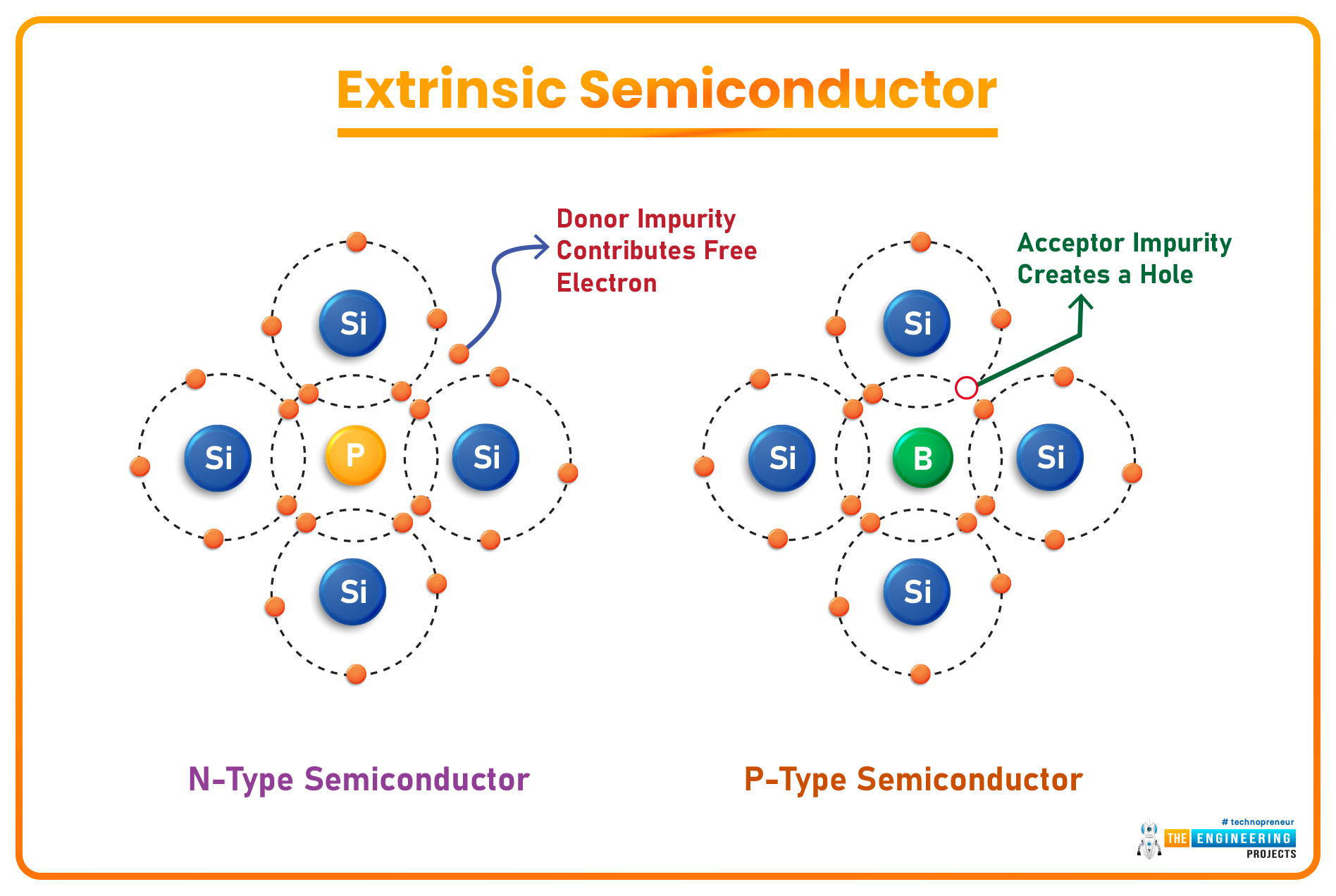
Extrinsic Semiconductor
- In order to increase the conductive power of semiconductors, small amounts of impurities(in the ratio of 1 to 106) are added to them, by a method called Doping.
- Such doped/impure semiconductors are called Extrinsic Semiconductors.
- Impurities added in the semiconductors are of two types i.e.
- Pentavalent (Arsenic, Antimony, Phosphorous etc.).
- Trivalent (Aluminium, Boron, Indium, Gallium etc.)
- If the semiconductor is doped with a Pentavalent impurity, it's called N-Type Semiconductor.
- If the doping element used is trivalent, the extrinsic semiconductor produced will be called P-Type Semiconductor.
So, now we need to understand the formation of N-Type and P-type semiconductors, because PN Junction is formed by joining these two types.
N-Type Semiconductors
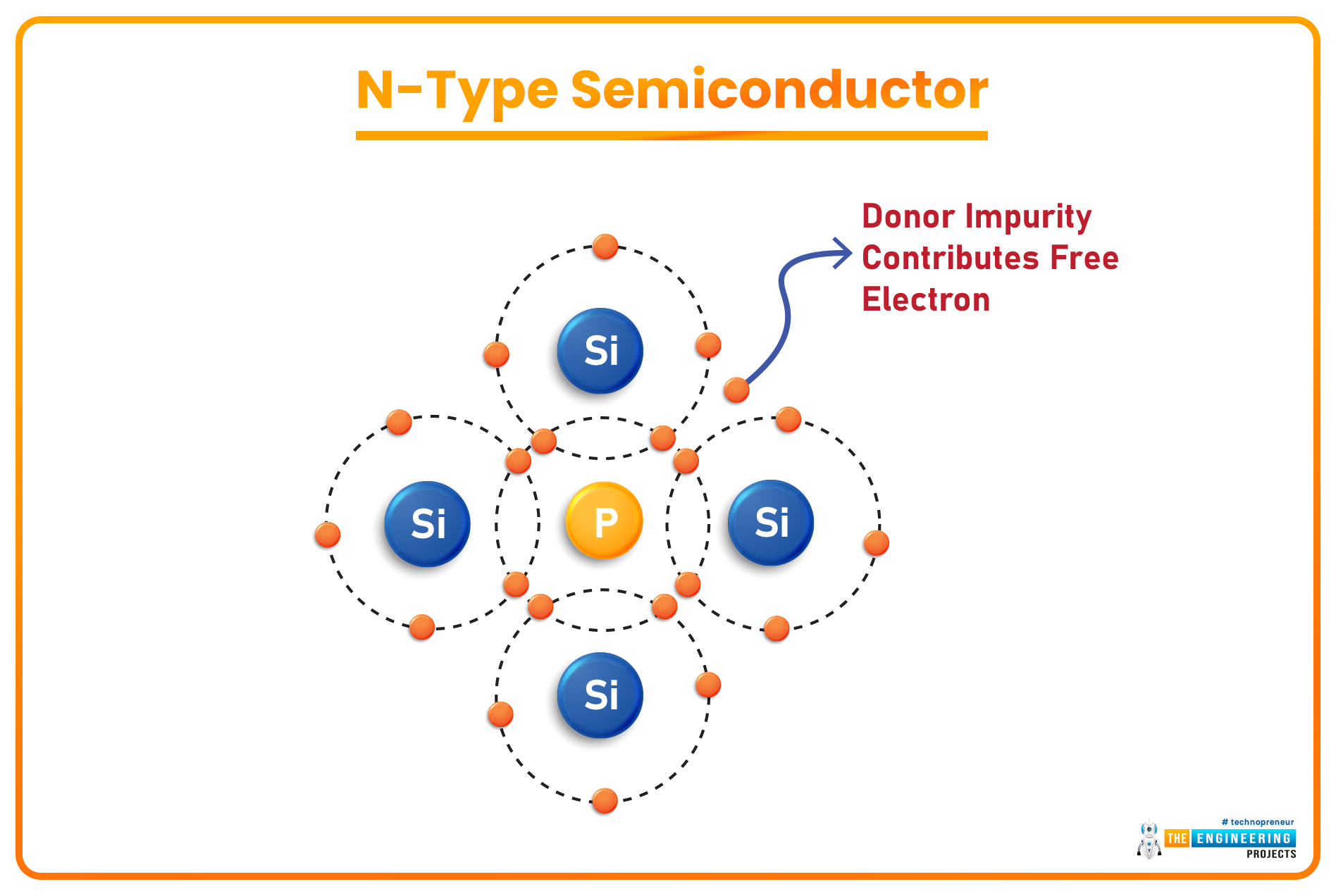
- Pure semiconductors normally belong to the 4th column of the periodic table and thus have an equal number of electrons & holes in their valance shell(which is 4).
- So, in pure form, there's no free electron or hole available for the conduction of electricity and thus it acts as an insulator. (We discussed conduction energy levels in detail in our last lecture)
- The pentavalent elements belong to the 5th column of the periodic table and have 5 electrons in their outermost shell.
- So, when a pure semiconductor i.e. Silicon(Si) is doped with a pentavalent impurity i.e. Boron(B), the four valance electrons of the Boron(B) will create a covalent bond with the closest Silicon(Si) atoms, but the 5th electron won't find a pair and will become a free electron.
- This free electron increases the conductive ability of the semiconductor.
- As an electron carries a negative charge, such extrinsic semiconductors are called Negative-Type Semiconductors or N-Type Semiconductors.
- In N-Type Semiconductors, the majority charge carriers are free electrons(negative), while the holes(positive) are present in very small numbers(called minority charge carriers).
Now let's have a look at the formation of P-Type Semiconductors:
P-Type Semiconductors
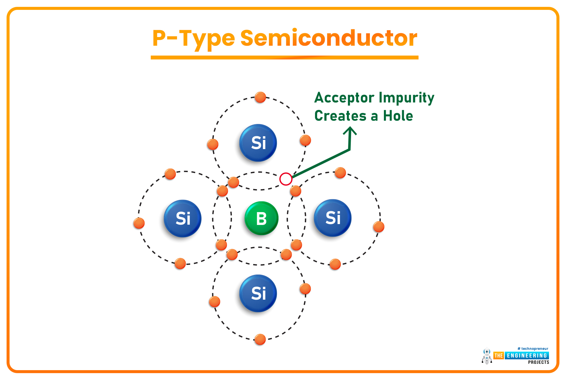
- When a semiconductor is doped with a trivalent impurity i.e. Aluminium(Al), the extrinsic semiconductor produced is called P-Type Semiconductor and has positively charged holes as majority charge carriers.
- Trivalent elements belong to the 3rd column of the periodic table and have 3 electrons in their outermost shell(valence shell).
- So, if we dope Silicon(Si) with Aluminium(Al), the 3 valence electrons of the impurity element(Al) will create a covalent bond with the neighboring Silicon(Si) atoms.
- The 4th valence electron of Si won't find a pair and thus a positively charged Hole will be originated. A Hole is a vacant space, has a positive charge and is ready to accommodate an electron(if available).
- This Hole generated in the Si crystal will increase its conductivity and such doped semiconductor will be called Postive-Type Semiconductor or P-Type Semiconductor.
So far, we have created N-Type and P-Type Semiconductors by adding pentavalent and trivalent impurities respectively in separate semiconductor crystals. Now, we are going to add both impurities in a single semiconductor crystal to create a PN Junction. So let's get started:
What is PN Junction?
- When a single crystal of semiconductor is doped with both pentavalent(i.e. Boron) and trivalent(i.e. Aluminium) impurities, a special barrier is created at the boundary of the two regions(N-Type & P-Type) which stops the flow of charge carriers. This barrier is called PN Junction.
- The most basic semiconductor component called Diode is a real-life application of the PN Junction.
Now let's have a look at the formation of this PN Junction:
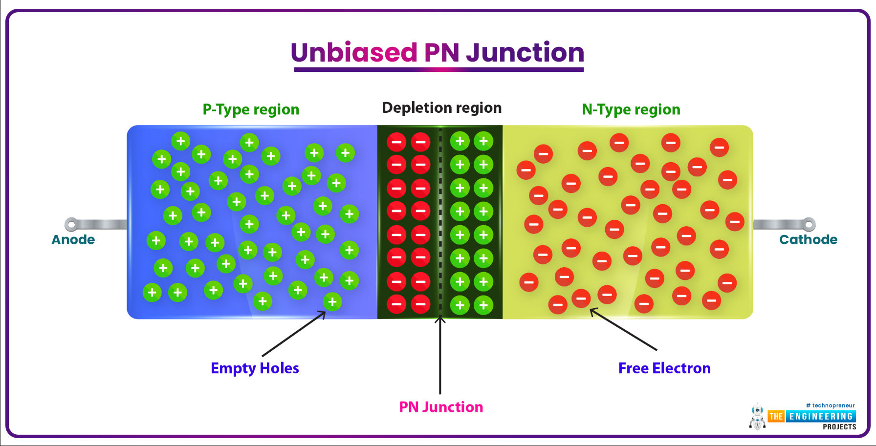
PN Junction Formation
- As we know, electrons are the majority charge carriers in N-Type Semiconductors and Holes are the majority charge carriers in P-Type Semiconductors.
- Now, when we dope a single Si crystal with both impurities, an N-Typer region is created on one side and a P-Type region is created on the other side of the crystal.
- Electrons(in the N-Type region) present near the boundary get excited and diffuse into the P-Type region. Similarly, the Holes(in the P-Type region) close to the boundary move towards the N-Type region.
- This generates a potential difference at the boundary of the two regions, which gradually increases and at one point, restricts the further flow of electrons or holes in the neighboring region. (electron-hole diffusion stops)
- This region at the boundary with electrons in the P-Type region and Holes in the N-Type region is called the depletion region.
- The width of this depletion region depends on the amount of impurity added to the semiconductor.
- This Junction/boundary of the P-Type and N-Type regions is called the PN Junction.

- Under normal conduction, when there is no voltage applied across the PN junction, the junction is said to be in an equilibrium state. The potential difference at the junction in that state is called built-in potential which is 0.7 V for Silicon(Si) and 0.3 V for Germanium(Ge).
- When an external voltage is applied at the PN Junction, we get two behaviors of PN Junction depending on the external voltage polarity, named:
- Forward-Biased.
- Reverse-Biased.
Let's discuss these diode states, one by one:
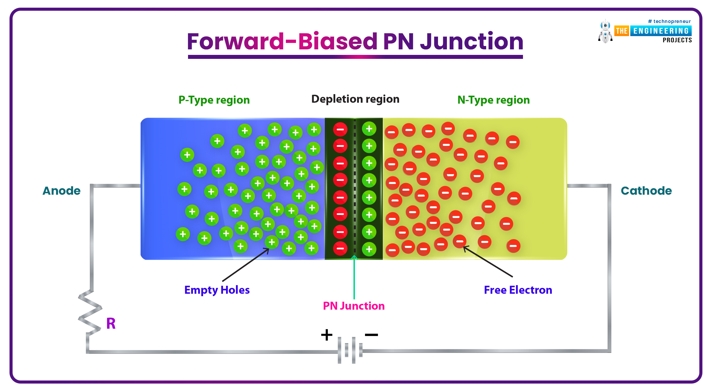
Forward-Biased PN Junction
- If the positive terminal of the battery is connected to the P-region and the negative terminal to the N-region, the PN Junction will be said to be operating in a Forward-Biased State.
- The external voltage should be greater than the built-in potential i.e. 0.7V for Si and 0.3V, so that it could melt the depletion region.
- In the Forward-Biased State, the Holes start to move towards the N-region and the electrons start flowing towards the P-region.
- As a result, the width of the depletion region starts reducing and finally depletes out.
- The current starts flowing through the semiconductor, as soon as the depletion region gets removed. We can say the semiconductor is acting as a conductor.
- In this state, the semiconductor has maximum conductivity and quite low resistance.

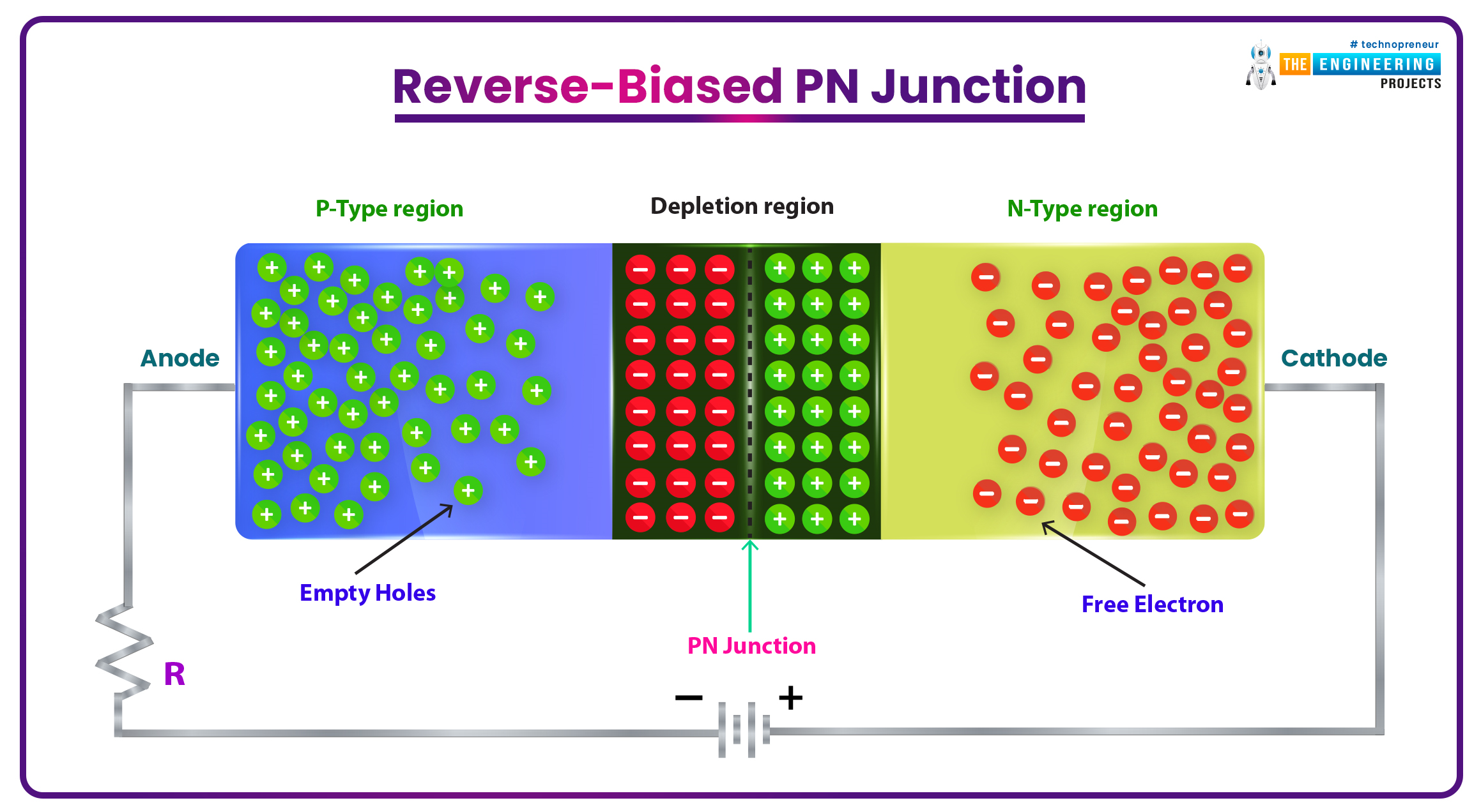
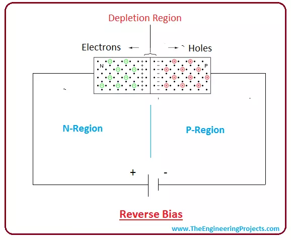
Reverse-Biased PN Junction
- If the P-region is connected with the negative terminal of the external source and the N-region with the positive terminal, the PN-Junction will operate in the reverse-biased state.
- As the P-region is connected to the negative voltage, the holes in the P-region will get attracted towards the external voltage, so start flowing away from the depletion region. The same will be the case with the electrons.
- So, no current will flow through the PN Junction in a reverse-biased state.
PN Junction as a One-Way Switch
In a normal conductive wire, current can flow in both directions but in a PN Junction, the current will flow only in one direction and will get blocked in the opposite direction. So, we can say that a PN-Junction is a One-Way Switch, allowing the current to flow in one direction only. On the top of my head, it could be used to avoid the back emf generated by the motors. This One-way switch literally bought a revolution in electronics.
Breakdown Region
- While the PN Junction is operating in the reverse-biased state, if the external voltage exceeds a certain limit, the PN Junction will collapse, resulting in an excessive amount of current flow(short-circuit). This external voltage is called breakdown voltage and the PN Junction is said to be operating in a breakdown region.
- PN Junction can't recover from the breakdown region so it should be avoided, though it also has a few advantages, which we will cover in the Zener Diode Chapter.
- The breakdown voltage depends on the semiconductor used and the amount of impurity added.
Characteristic Curve of PN Junction
The following figure shows the I vs V characteristic curve of a silicon diode:
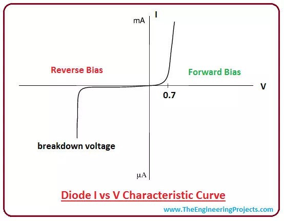
- As we can see in the above characteristic curve of PN Junction, it has two sections i.e. forward-biased and reverse-biased.
- In the forward-biased state, if the voltage is lower than the built-in potential(i.e. 0.7 for Si), a small amount of current is flowing through the PN Junction but if the voltage overcomes the built-in potential, the current jumps to its maximum value and we can say the PN Junction is conducting.
- In the reverse-biased state, there's no current flowing through the PN Junction until the breakdown voltage is reached.
- At the breakdown voltage, the current starts flowing in the opposite direction and we can say the PN Junction collapsed.
- The small current flowing under reverse bias normal condition is known as leakage current. Germanium(Ge) has more leakage current as compared to Silicon(Si).
So, that's all for today. I hope you have enjoyed today's lecture. In the next lecture, we will discuss the Basics of Diodes, where I am going to repeat today's lecture :)) But I will keep the practical approach in it, so there will be a lot to learn. If you have any questions, you can approach me in the comment section below. Keep your suggestions and feedback coming, they help us deliver quality content. Thanks for reading the article.
