Introduction to CD4047
Introduction to CD4047
CD4047 is a CMOS Low Power monostable/astable multivibrator mainly used for converting DC current signal to AC signal. It comes with a high voltage rating around 20-V.- CD4047 is a 14 pin IC that operates on a logic techniques with an ability to allow negative or positive edge-triggered monostable multivibrator action layered with retriggering and external counting options.

- There is a sheer difference involved when IC works in monostable and astable mode. In monostable mode, the inverter needs a trigger signal for generating the output pulse, but an astable multivibrator doesn't require trigger signal for every output pulse. More often than not, an astable multivibrator can be called as an oscillator.
CD4047 Features
No matter what type of operation this IC undergoes, an external resistor is permanently connected between RC-Common and R timing terminals and an external capacitor is connected between RC-Common and C timing terminals. The following figure shows the main features of this IC.| Features |
|---|
| Low Power Consumption Noise Resistance Generate both Monostable and Astable operation Symmetrical buffered output characteristics One resistor and one capacitor is used externally |
| Monostable Features |
| Output pulse width doesn't dependent on trigger pulse duration Pulse width expansion with retrigger option The positive and negative edge trigger option is available |
| Astable Features |
| Creates 50% duty cycle Free running operating modes Oscillator output Impressive frequency stability |
CD4047 Pinout
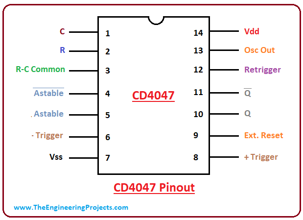
Following figure shows the pinout diagram of CD4047.
- There are 14 pins available on the IC where Vss is a ground pin and Vdd is a voltage supply pin. There are six inputs including trigger', trigger, astable, astable', external reset and retrigger. While buffer outputs include three outputs mentioned as Q, Q', and Oscillator.
- The IC behaves as a gatable multivibrator if complement pulses on the astable' and true pulses are applied on the astable pins.
CD4047 Pin Description
As mentioned earlier there are 14 pins on the IC interface with every pin is used with a specific purpose. Folloiwng table shows the pin description of each pin.| Pin# | Pin Name | Pin Description |
|---|---|---|
| 1 | C | Connected to an external capacitor |
| 2 | R | Connected to an external resistor |
| 3 | R-C Common | Common pin for establishing a connection with resistor and capacitor |
| 4 | Astable' | Must be kept low when used in astable mode |
| 5 | Astable | Must be kept high when used in astable mode |
| 6 | -Trigger | High to Low transition will be given to this pin when used in Monostable mode |
| 7 | Vss | Ground Pin |
| 8 | +Trigger | Low to high transition will be given to this pin when used in Monostable mode |
| 9 | EXT Reset | External reset triggers when a high pulse is provided to this pin, resetting the output Q to low and Q’ to high |
| 10 | Q | Generates high output |
| 11 | Q' | It is an inverse output of pin 10, producing a low output |
| 12 | Retrigger | This pin is used in Monostable mode for simultaneously retriggering +trigger and –trigger pin |
| 13 | Osc Out | Generate oscillated output |
| 14 | Vdd | Voltage supply pin |
CD4047 Working in Monostable and Astable Mode
CD4047 is a low power inverter that comes with an ability to operate in both states: astable or monostable mode. In astable mode, it operates by charging a capacitor using a valuable resistor that is mainly used to adjust the output frequency near 50Hz. Monostable Mode In Monostable Mode, an external resistor must be connected between Pin 1 & 3 of the IC that helps in determining the output pulse width. We will be using +trigger and –trigger Pin in this mode.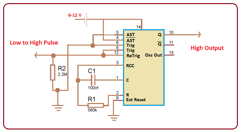
f = 1 / 8.8 x R*C
Astable mode As mentioned earlier in astable mode, the inverter needs a trigger signal for generating the output pulse. The output frequency is determined when a single capacitor is connected between PIN 2 and 3.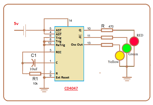
F = 1 / 4.4 x R*C
Similarly, the formula to find the time it takes to generate pulse will be given as:t = 2.48 x R*C
Applications
This inverter comes with a wide range of applications that are mainly related to DC to AC conversion. Following are the main applications it can be used for.- Frequency division
- Frequency multiplication
- Timing delay applications
- Timing circuits
- Frequency discriminators
×
![]()


