IRF840 MOSFET Datasheet, Pinout, Features, Equivalent & Applications

Hi Fellas! I hope you’re well today. Happy to see you around. In this post today, I’ll walk you through the Introduction to IRF840.
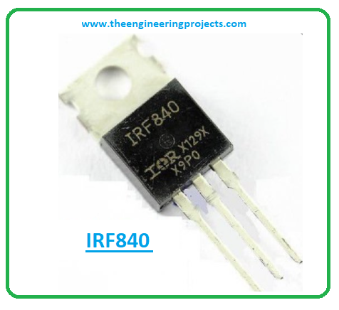
The IRF840 is an n-channel power MOSFET. It is a fast switching and high voltage device that is available with low on-state resistance. As this is an n-channel MOSFET here conduction process is exercised by the movements of the electrons. In other words, though conduction is carried out by both the movement of holes and electrons, electrons are major carriers in this case.
I suggest you read this entire post till the end as I’ll discuss the complete Introduction to IRF840 covering datasheet, pinout, features, equivalent, and applications. Let’s jump right in.
Introduction to IRF840
- The IRF840 is an n-channel power MOSFET that supports loads up to 8A and 500V. It is a fast-switching and high-voltage device that requires 10V across the gate terminal to initiate the conduction process.
- This IRF840 MOSFET is a three-terminal device made of gate (G) drain (D) and source (S) terminals. The external circuits are connected with these MOSFETs through these terminals.

- This is an N-channel MOSFET, here the conduction process is exercised by the flow of electrons in contrast to the P-channel MOSFET where the conduction process is carried out by the flow of holes.
- It is important to note that conduction is a process that is carried out inside MOSFET by the movements of both electrons and holes but electrons are major carriers in the n-channel MOSFET devices while holes are major carriers in the p-channel MOSFET devices.

- The MOSFET stands for Metal Oxide Silicon Field Effect Transistor. It is also known as the IGFET Insulated Gate Field Effect Transistor. It is made by the controlled oxidation of a silicon semiconductor material.
- MOSFETs and BJTs (bipolar junction transistors) are considered as different semiconductors as BJT is a current-controlled device while the MOSFET is a voltage-controlled device.
- The voltage applied at the gate terminal usually is directly related to the current between the source and drain terminals. The gate terminal voltage controls the current at the drain and source terminals. Simply put, the gate terminal acts like a control valve that controls the current between two terminals.

IRF840 Datasheet
Before incorporating this device into your electrical project, it’s better to scan through the datasheet of the component that features the main characteristics of the device. You can download the datasheet of this component IRF840 by clicking the link given below.
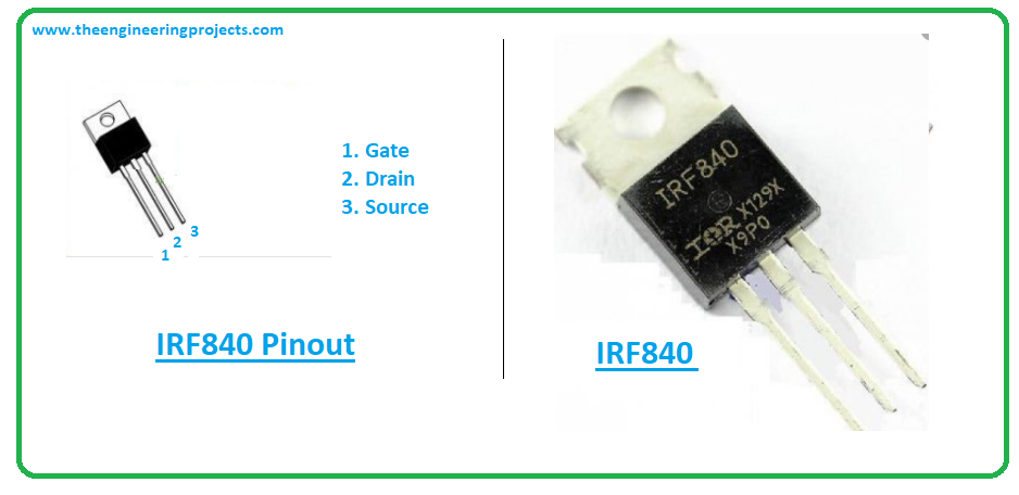
IRF840 Pinout
The IRF840 is an N-channel power MOSFET. It is a fast-switching device that comes with three pins known as:
- Gate
- Drain
- Source
Recall, the gate terminal controls the current between the source and drain terminals. The gate terminal initiates the conduction process when we apply the biased voltage of around 10V at the gate terminal.
The following figure shows the pinout diagram of IRF840 MOSFET.
Mind it… generally, the MOSFET is a four-pin component that contains four terminals called:
- Source (S)
- Gate (G)
- Drain (D)
- Body (B) / Substrate.
The bodyside is always connected with the source pin. So we generally call the MOSFET a three-terminal device.
IRF840 Features
- Type: N-Channel fast switching Power MOSFET
- The rise time and the fall time are 23nS and 20nS respectively
- Gate threshold voltage (VGS-th) = 10V (limit = ±20V)
- Continuous Drain Current (ID) = 8A
- Drain Source Resistance (RDS) = 0.85 Ohms
- Available package = TO-220
- Drain to Source Breakdown Voltage = 500V
IRF840 Equivalent
The following are the equivalent of IRF840.
- 8N50
- FTK480
- KF12N50
IRF840 Applications
The IRF840 is used in the following applications.
- Used in Inverter Circuits and DC-DC Converters.
- Incorporated in High-Speed switching applications.
- Used for switching high-power devices.
- Employed in Control speed of motors and LED dimmers or flashers.
That was all about the Introduction to IRF840. Hope you enjoyed reading this article. If you’re unsure or have any questions, you can pop your query in the section below. I’d love to help you the best way I can. You’re most welcome to share your thoughts about the content we share so we keep sharing quality content based on your needs and requirements. Thank you for reading the article.


