LF353N Dual JFET Input Op-Amp Datasheet, Pinout, Features & Applications

Hi Folks! I hope you’re well today. I welcome you on board. Happy to see you around. In this post today, I’ll walk you through the Introduction to LF353N.
The LM393N is a wide bandwidth and high input impedance Dual Input JEFET op-amp that is widely used in high-speed integrators and low noise circuits. The low bias current and input noise make it a good pick for audio amplifier applications. It carries a high slew rate (13V/uS) and wide bandwidth around (4MHz).
I suggest you read this post all the way through, as I’ll detail the complete introduction to LF353N covering datasheet, pinout, features, and applications. Let’s dive in.
Introduction to LF353N
- Introduced by the Texas Instrument, the LM393N is a high input impedance dual op-amp where the input of this device is attached through a high voltage JFET.
- It is widely used in low current, low noise fast switching applications.
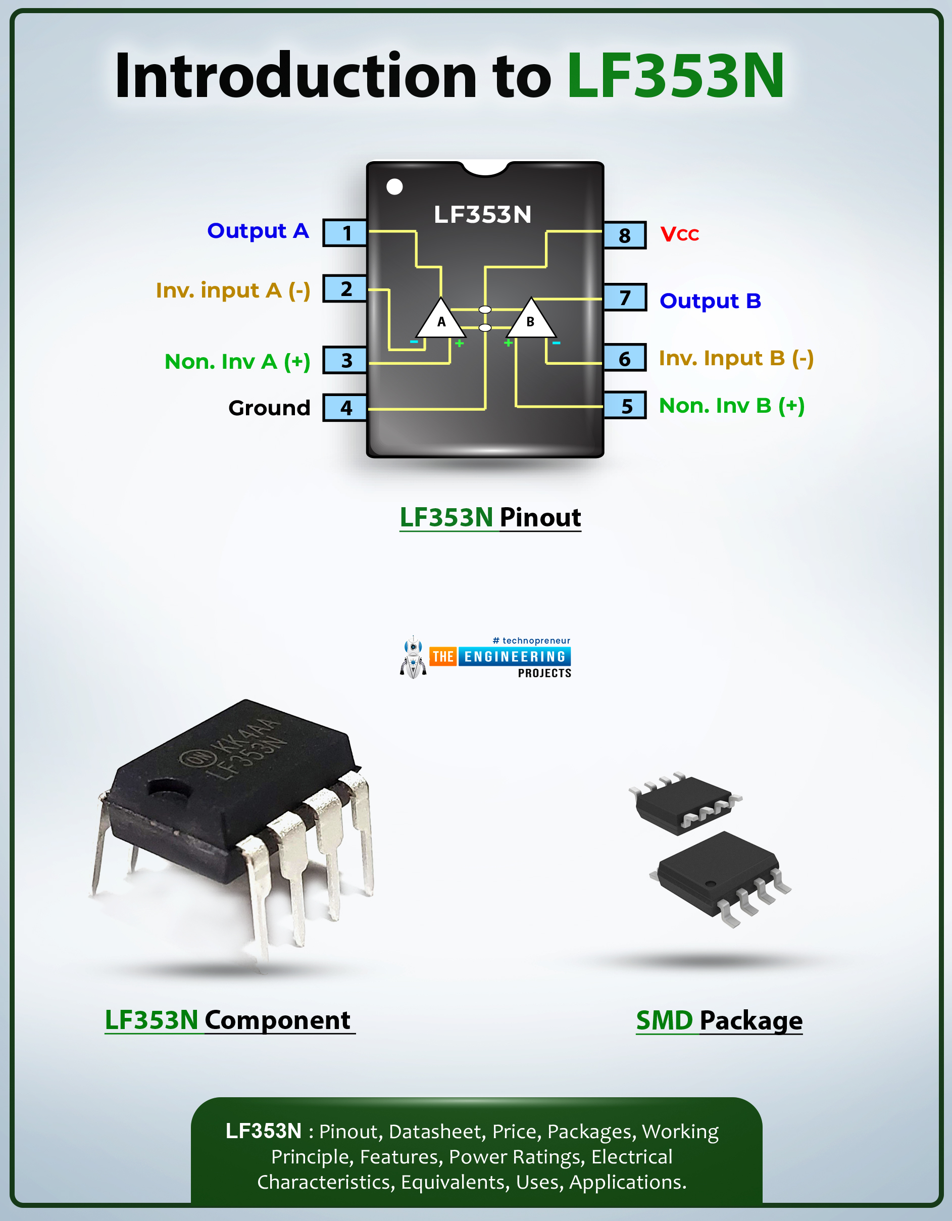
- There are two outputs available on the device i.e. Output A and Output B. And two inputs where each input contains further two inputs i.e. inverting input (-) and non-inverting input (+).
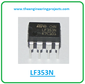
- This chip incorporates two independent op-amps that operate over a wide range of voltages from a single power supply.
- High slew rate and high input impedance device, LF353N comes with internally compensated input offset voltage.
- It is also available with a power supply voltage range of ±18 V and with a differential input voltage of around 30V.
- The power dissipation Pd is 500mW which is defined as the maximum energy dissipated during the working of this device.
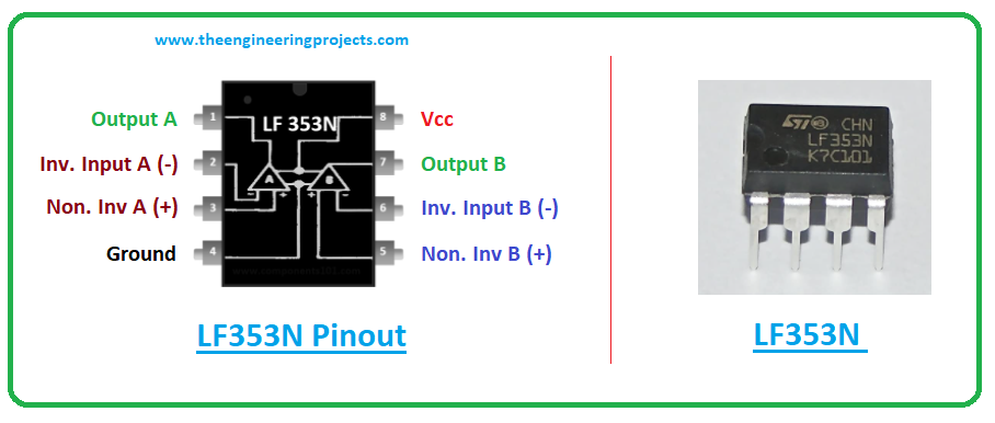
LF353N Datasheet
Before you incorporate this device into your electrical project, it’s wise to scan through the datasheet of the component that features the main characteristics of the component. Click the link below to download the datasheet of LF353N.LF353N Pinout
The following figure shows the pinout diagram of LF353N.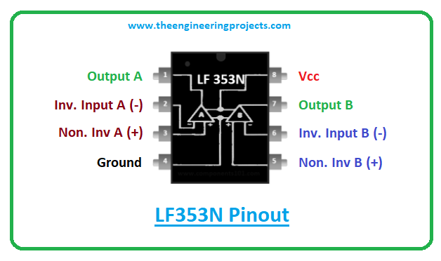
| Pin Description of LF353N | ||||
|---|---|---|---|---|
| Pin No. | Pin Description | Pin Name | ||
| 1 | The output of Op-Amp 1 | OUT (A) | ||
| 2 | Inverting Input of Op-Amp 1 | INPUT- A(-) | ||
| 3 | Non-Inverting Input of Op-Amp 1 | INPUT- A(+) | ||
| 4 | Ground or Negative supply terminal | Power (-Vs) | ||
| 5 | Non-Inverting Input of Op-Amp 2 | INPUT- B(+) | ||
| 6 | Inverting Input of Op-Amp 2 | INPUT- B(-) | ||
| 7 | The output of Op-Amp 2 | OUTPUT B | ||
| 8 | Positive supply terminal | +Vcc | ||
LF353N Features
- Dual Op-Amp that comes with JFET Input
- High slew rate 13V/µs
- High Input Impedance 1012?
- Low Input Noise current
- Low input noise voltage
- Supply Current = 6.5mA (max)
- Bandwidth Gain = 4MHz
- Supply Voltage = ±18V
- Available Packages = 8-pin SOIC & PDIP Package
LF353N Equivalent
The following are the equivalents of LF353N.- LM1558
- TL074
- MCP6002
While working with the alternatives, make sure you cross-check the pinout of them. It’s quite likely the pinout of the alternatives might differ from the pinout of LF353N.
LF353N Applications
The LF353N is used in the following applications.
- Used in High-Input Impedance designs
- Employed in Low-noise Audio circuits
- Used in High-Speed Integrator
- Incorporated in Sample and Hold Circuit
That’s all for today. I hope you’ve loved reading this article. If you have any questions, you can approach me in the section below, I’d reply to you according to the best of my experience. Feel free to share your valuable suggestions and feedback around the content we share, so we keep producing quality content customized to your needs and requirements. Thank you for reading this article.


