


MJE13005 NPN Transistor Datasheet, Pinout, Features & Applications


Hi Guys! I welcome you on board. Thank you for clicking this read. In this post today, I’ll walk you through the Introduction to MJE13005. The MJE13005 is a high speed and high voltage power transistor that belongs to the NPN transistor family. This device can support load up to 4A and the emitter-base voltage is 9V which is the voltage required to bias the device and start the transistor action. I suggest you read this post all the way through as I’ll detail the complete Introduction to MJE13005 covering datasheet, pinout, features, and applications. Let’s get started.
Introduction to MJE13005
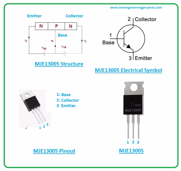
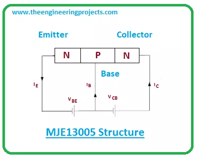
- The MJE13005 is an NPN transistor which is a high speed and high power device used for amplification and switching purposes.
- This component is made of three-layers where one is p-doped layers and the other two are n-doped layers. The p-doped layer stands between these two n-doped layers.
- The MJE13005 is a semiconductor device made of silicon material. It contains three terminals known as emitter, base, and collector and is termed as a current-controlled device as opposed to MOSFETs which are voltage-controlled devices and contain terminals source, drain, and gate.
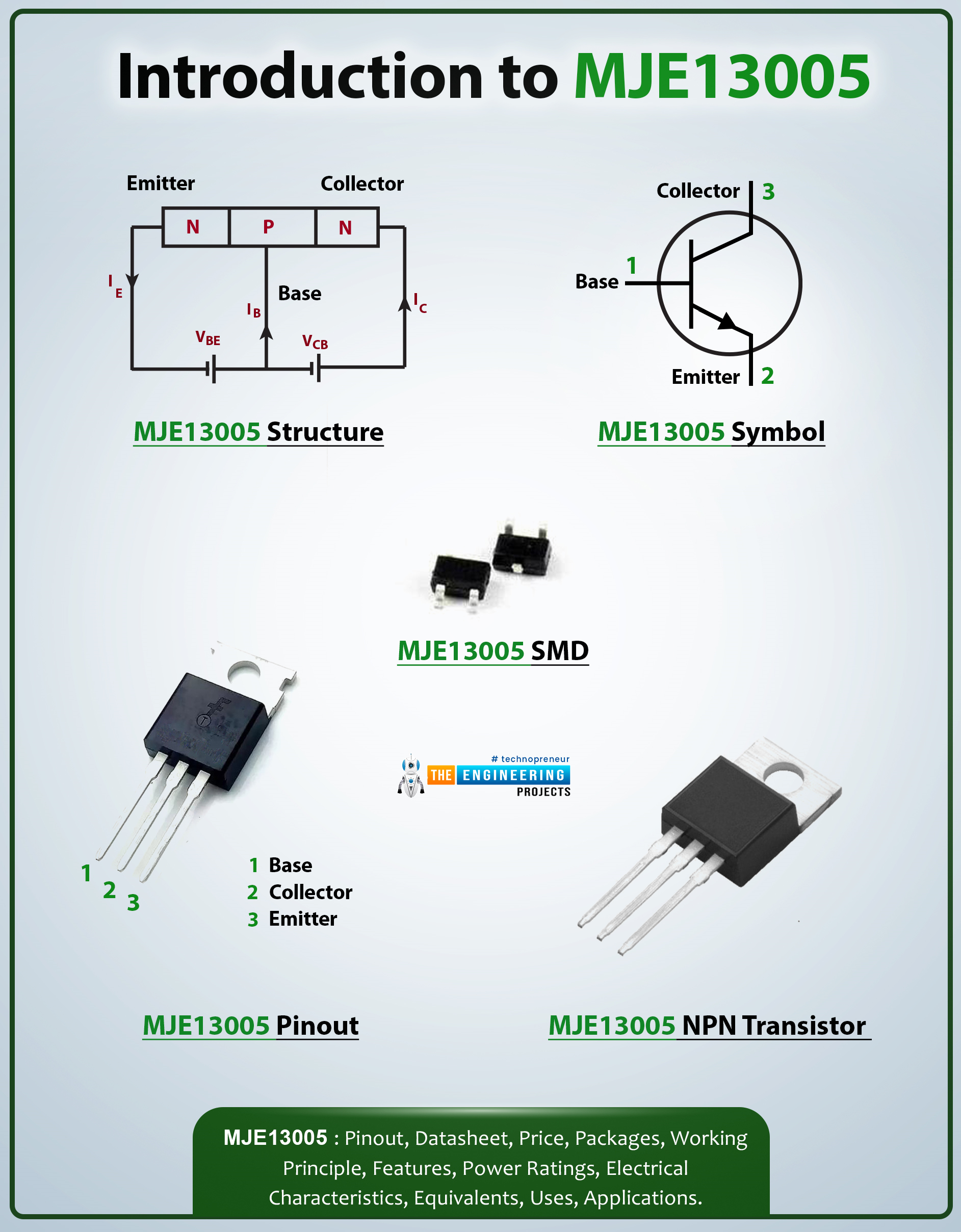
- All these terminals carry different doping concentrations. The doping concentration of the collector pin is light and the doping concentration of the emitter pin is high compared to the other two terminals. The base pin is 10-times more doped than the collector pin. Moreover, the emitter side carries the entire current of the device since the emitter current is the sum of both collector current and base current.
- The bipolar junction transistors are mainly categorized into two types i.e. NPN transistors and PNP transistors.
- Both electrons and holes play a vital role in conductivity in both these transistors. But in the case of NPN transistors holes are the majority carriers and in the case of PNP transistors holes are majority carriers.
- The NPN transistors are preferred over PNP transistors for a range of applications because the mobility of electrons is better than the mobility of holes.
- NPN devices are sometimes known as “sinking devices” since they sink ground to the output. PNP devices are sometimes named “sourcing devices” since they source positive power to the output.
- The DC current gain of this device ranges from 8 to 40 which is the amount of current this device can amplify.
MJE13005 Datasheet
Before you embed this device into your electrical project, it’s wise to scan through the datasheet of this component that features the main characteristics of the device. Click the link below to download the datasheet of MJE13005.MJE13005 Pinout
The following figure shows the pinout diagram of MJE13005.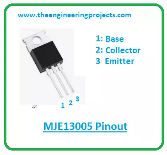
- Base
- Collector
- Emitter
MJE13005 Working Principle
- The working of this device starts from the base pin. When voltage is applied at the base pin, it results in biasing the device, and current starts flowing from collector to emitter terminal.
- Know that these bipolar junction transistors are not symmetrical devices. This means if we exchange both emitter and collector terminal, it prevents both these terminals to work in forward active mode and as a result, both these terminals will start working in reverse active mode. Doing this will affect the values of common-emitter current gain and common-base current gain.
- This lack of symmetry comes from the different doing concentrations of all three terminals.
- The Common-emitter current gain of this device ranges from 8-40 in this device, which is denoted by beta and the common-base current gain is denoted by alpha and is always less than one.
MJE13005 Equivalent
The following are the alternative to MJE13005:- KSE13007
- MJE13007
- 2SC3795
MJE13005 Power Ratings
The following table shows the absolute maximum ratings of MJE13005.| Absolute Maximum Ratings of MJE13005 | ||||
|---|---|---|---|---|
| Pin No. | Pin Description | Pin Name | ||
| 1 | Collector-emitter voltage | 400V | ||
| 2 | Collector-base voltage | 700V | ||
| 3 | Base-emitter voltage | 9V | ||
| 4 | Collector current | 4A | ||
| 5 | Power dissipation | 70W | ||
| 6 | Base current | 2A | ||
| 7 | Operating and storage junction temperature range | -55 to 150C | ||
MJE13005 Applications
MJE13005 is embedded in the following applications.- Used in voltage regulator circuits.
- Used in H-bridge circuits.
- Incorporated in modern electronic circuits.
- Used in Bistable and Astable multivibrators circuit.
- Employed to support loads under 4A.
- Used for switching and amplification purpose.
- Installed in the motor control circuit.
- Employed in the switched-mode power supply.
MJE13005 Physical dimensions
The following figure represents the physical dimensions of the MJE13005 device.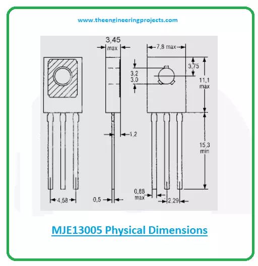
×
![]()


