2SC2240 Datasheet, Pinout, Power Ratings, Equivalents & Applications
Hello Everyone! Happy to see you around. In this post today, we’ll cover the 2SC2240 NPN Transistor. We will have a look at the 2SC2240 Datasheet, Pinout, Power Ratings, Equivalents & Applications.
Electrons are the majority charge carriers in this NPN transistor, in contrast to PNP transistors, where holes are the majority carriers. The 2SC2240 comes with a power dissipation of 0.3W, the amount of energy this transistor dissipates while operating in the forward-biased state, while the collector current is 0.1A means it can support load up to 0.1A.
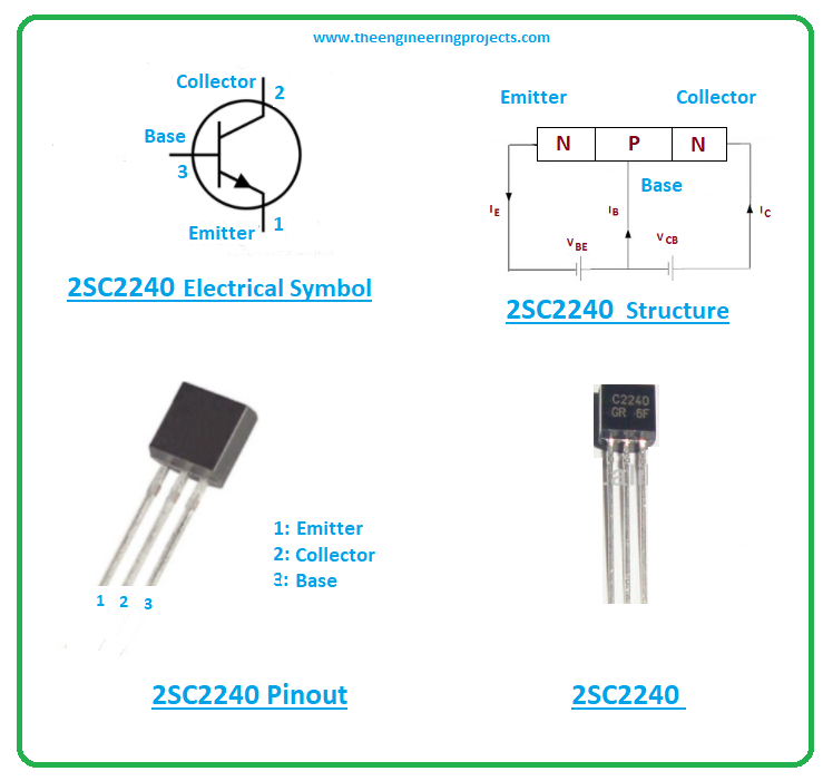
This NPN transistor contains 3 terminals, named:
- Emitter
- Collector
- Base
If the voltage at the base terminal is above 0.7V, the transistor will get forward-biased and the current will start flowing from Collector to Emitter terminal. If the base voltage is less than 0.7V, it will remain reverse-biased.
So, let's have a look at the 2SC2240 NPN Transistor in detail. Let’s get started:
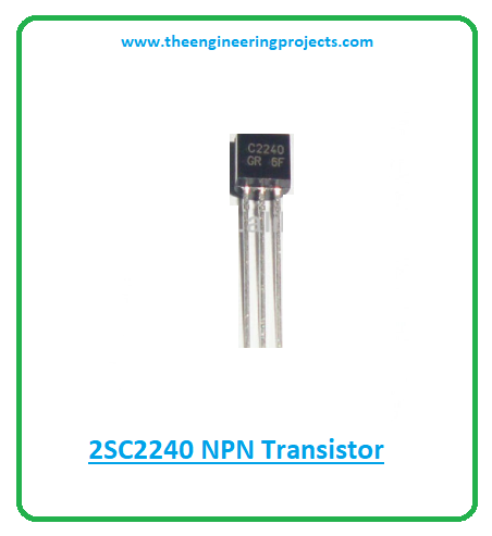
2SC2240 NPN Transistor
- The 2SC2240 is a bipolar junction transistor that belongs to the NPN transistor family.
- This component is mainly used for switching and amplification purposes and comes in a TO-92 package.
- 2SC2240 comes with three layers, with one p-doped layer between two n-doped layers.
- The two n-doped layers represent the Collector and Emitter, while the p-doped layer represents the Base Terminal.
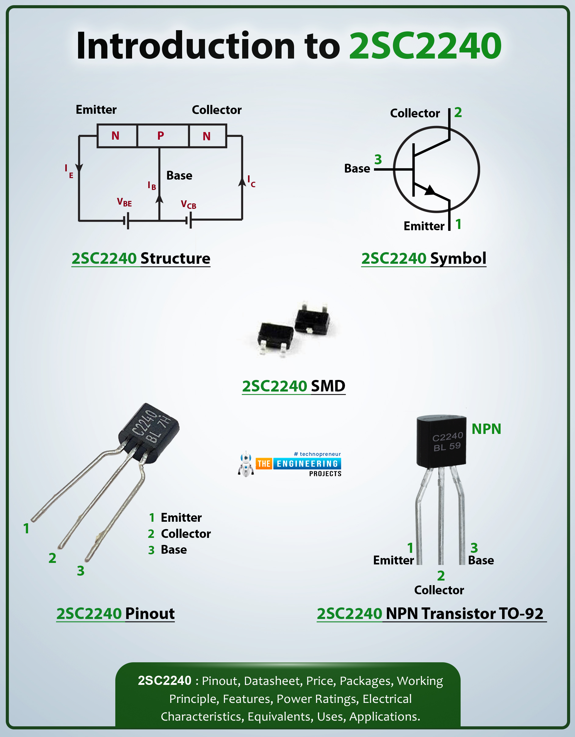
- This device contains three terminals: the base, collector, and emitter. The collector terminal collects the electrons coming from the base side and the emitter terminal emits the electrons into the base terminal.
- The NPN transistors contain two junctions known as collector-base junction and emitter-base junction.
- The transistor is said to operate in a Forward-Biased state, when the collector-base junction is reverse-biased, while the emitter-base junction is forward-biased.
- When a negative voltage is applied at the emitter side and a positive voltage is available at the base terminal then we can make the emitter-base junction forward biased.
NPN vs. PNP: A Quick Recall
- Bipolar Junction Transistors(BJTs) are categorized into two types i.e. NPN transistors and PNP transistors. This is a bipolar transistor, which means both electrons and holes play a role in the conductivity process inside the transistor.
- But electrons are the major carriers in NPN transistors while in the case of PNP transistors, holes are the major carriers.
- NPN transistors are preferred over PNP transistors because the mobility of electrons is more efficient than the mobility of holes.
- These bipolar devices are called current-controlled devices, in opposition to MOSFETs, which are called voltage-controlled devices and carry terminals like a drain, source, and gate.
2SC2240 Datasheet
It’s wise to go through the 2SC2240 datasheet before you apply this device to your electrical project.
2SC2240 Pinout
The following figure shows the 2SC2240 pinout.
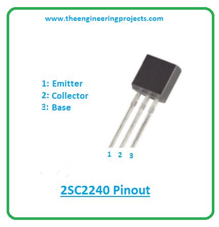
This component contains three terminals named: 1: Emitter 2: Collector 3: Base
- These terminals differ in terms of size and doping concentration and are used for external connection with the electronic circuit. The emitter side is highly doped and the base side is lightly doped and the collector terminal is moderately doped.
- The collector terminal dissipates more energy compared to the other two terminals. It is bigger in size compared to base and emitter terminals. The large surface area of the collector side guarantees more heat dissipation.
2SC2240 Working Principle
The base is responsible for the transistor action. When voltage is applied at the base terminal, it will bias the device and as a result, the current will flow from collector to emitter terminal. As this is an NPN transistor so here current will flow from the collector to the emitter side and in the case of the PNP transistor current will flow from the emitter to the collector side.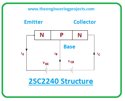
2SC2240 Power Ratings
The following table shows the 2SC2240 power ratings.| Absolute Maximum Ratings of 2SC2240 | ||||
|---|---|---|---|---|
| Pin No. | Pin Description | Pin Name | ||
| 1 | Collector-emitter voltage | 120V | ||
| 2 | Collector-base voltage | 120V | ||
| 3 | Base-emitter voltage | 5V | ||
| 4 | Collector current | 0.1A | ||
| 5 | Power dissipation | 0.3W | ||
| 6 | Current gain | 200 to 700 | ||
| 7 | Operating and storage junction temperature range | -55 to 125C | ||
- If these ratings are applied more than the required time, they can affect the device reliability.
- The collector-current is 0.1A which defines the amount of load this component can support.
- The power dissipation is 0.3W which represents the amount of energy released during the working of this component.
- The current gain ranges from 200 to 700 which is the amount of current this device can amplify.
- The operating and storage junction temperature ranges from -55 to 125C.
- The emitter-base voltage is 5V represents the voltage required to bias this component. The collector-base voltage and collector-emitter voltage both are 120V.
- When using this device, make sure these ratings don’t exceed the absolute maximum ratings else they can damage the device.
2SC2240 Equivalents
The following are the 2SC2240 equivalents.- 2SC3201
- 2SC3245A
- 2SC3200
- 2SC3245
- 2SC2459
- KTC3200
2SC2240 Applications
The following are the 2SC2240 applications.- Incorporated in modern electronic circuits.
- Used in Bistable and Astable multivibrators circuit.
- Used in voltage regulator circuits.
- Used in a common power amplifier.
- Used in electronic Ballasts.
- Used in energy-saving lights.
- Employed to support loads under 0.1A.
- Used in the high switching power supply.
- Used in high-frequency power transform.
2SC2240 Physical Dimensions
The following diagram shows the 2SC2240 physical dimensions.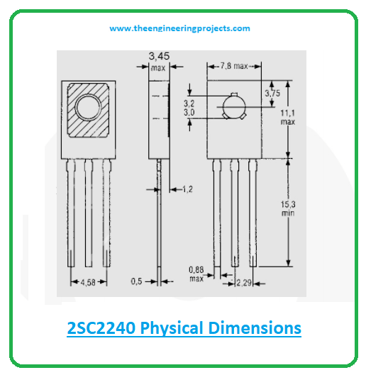
With physical dimensions, you can evaluate the space required for this device in the electrical project.
That’s all for today. Hope you find this article helpful. Feel free to share your valuable feedback and suggestions around the content we share. They help us produce quality content based on your needs and requirements. If you’re unsure or have any questions, you can approach men in the section below. I’m happy and ready to help you the best way I can. Thank you for reading this post.


