KSC1845 Datasheet, Pinout, Power Ratings, Equivalents & Applications

Hi Guys! I welcome you on board. In this post today, we’ll discuss the KSC1845 NPN Transistor. We will have a look at the KSC1845 Datasheet, Pinout, Power Ratings, Equivalents & Applications in detail. As it's an NPN transistor, electrons are the majority charge carriers and thus play a major role in conductivity. KSC1845 is mainly used for fast-switching and amplification purposes.
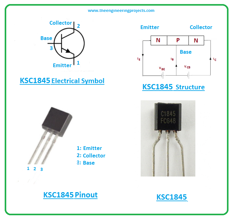
NPN transistor carries 3 terminals, known as:
- Emitter
- Collector
- Base
If the applied voltage at the base terminal exceeds 0.7V, it will forward bias this NPN transistor and the current will start to flow from Collector to Emitter. If the base voltage is less than 0.7V, KSC1845 will remain in the reverse-biased state.
I suggest you buckle up as I’ll discuss the KSC1845 NPN Transistor in detail. Let’s get started:
KSC1845 NPN Transistor
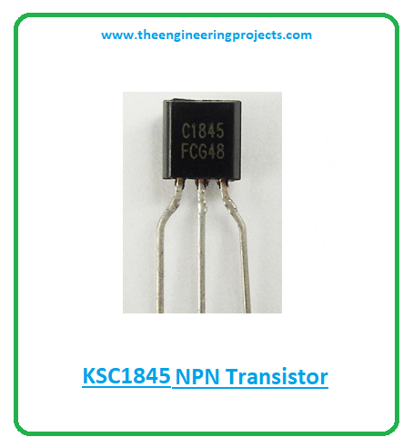
- The KSC1845 is a bipolar junction transistor that falls under the NPN transistor family.
- It is made of silicon semiconductor material and comes in a TO-92 package.
- The NPN transistors carry two junctions known as emitter-base junction and collector-base junction.
- When the emitter-base junction is forward-biased and the collector-base junction is reverse-biased, the transistor starts to conduct.
- KSC1845 Pinout, Symbol and SMD Package are shown in the below figure:
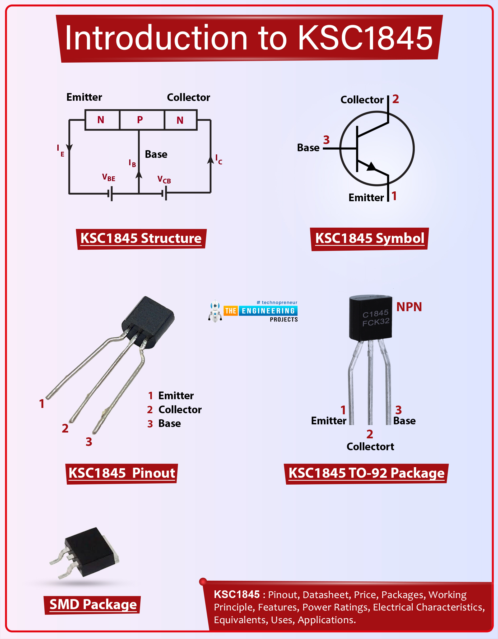
- We can make the emitter-base junction forward-biased, by applying a negative voltage at its Emitter and a positive voltage at its Base.
- KSC1845 contains three layers where one p-doped layer sits between two n-doped layers. The p-doped layer represents the base terminal while the other two n-doped layers represent Collector and Emitter.
- In a forward-biased state, the Emitter emits the electron into the Base while the Collector collects the electrons coming from the Base.
NPN vs PNP
KSC1845 is a Bipolar Junction Transistor, so let's quickly recall it:
- The bipolar junction transistors come in two types i.e. NPN transistors and PNP transistors. Both holes and electrons play a role in carrying out the conductivity process inside the transistor.
- In PNP transistors, holes are the majority charge carriers, while in NPN transistors, electrons are the majority charge carriers.
- Know that the mobility of electrons is better than the mobility of holes, that's why NPN transistors are preferred over PNP transistors for a range of applications.
- These bipolar(BJT) components are called current-controlled devices in opposition to MOSFETs, which are considered voltage-controlled devices and carry terminals like a drain, source, and gate.
KSC1845 Datasheet
Before you incorporate this device into your electrical project, it’s wise to go through the KSC1845 datasheet that details the main characteristics of the device. Click the link below to download the KSC1845 datasheet.
KSC1845 Pinout
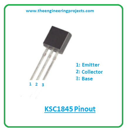
The following figure shows the KSC1845 pinout.
KSC1845 Working Principle
The base side is the main region that initiates the transistor action. When voltage is applied at the base terminal, it will bias the device and as a result, current starts flowing from collector to emitter side.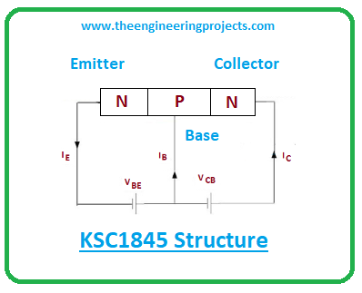
KSC1845 Power Ratings
The following table represents the KSC1845 power ratings.| Absolute Maximum Ratings of KSC1845 | ||||
|---|---|---|---|---|
| Pin No. | Pin Description | Pin Name | ||
| 1 | Collector-emitter voltage | 120V | ||
| 2 | Collector-base voltage | 120V | ||
| 3 | Base-emitter voltage | 5V | ||
| 4 | Collector current | 0.05A | ||
| 5 | Power dissipation | 0.5W | ||
| 6 | Current gain | 200 | ||
| 7 | Operating and storage junction temperature range | -55 to 150C | ||
- When using this device, make sure these ratings don’t exceed the absolute maximum ratings else they can damage the device.
- Plus, if these ratings are applied more than the required time, they can affect the device reliability.
- The collector-current is 0.05A which shows the amount of load this device can support.
- The power dissipation is 0.5W which represents the amount of energy released during the working of this component.
- The current gain is 200 which shows the amount of current this device can amplify.
- The collector-base voltage is 120V and the collector-emitter voltage is 120V. The emitter-base voltage is 5V represents the voltage required to bias this component.
KSC1845 Equivalents
The following are the KSC1845 equivalents.- FJV1845
Before applying alternatives into your projects, double-check the pinout of these alternatives as the pinout of KSC1845 might differ from the pinout of the equivalents.
The KSA992 is a complementary PNP transistor to the KSC1845.KSC1845 Applications
The following are the KSC1845 applications.- Incorporated in modern electronic circuits.
- Used in high-frequency power transform.
- Used in electronic Ballasts.
- Used in voltage regulator circuits.
- Used in a common power amplifier.
- Used in Bistable and Astable multivibrators circuit.
- Used in energy-saving lights.
- Employed to support loads under 0.05A.
- Used in the high switching power supply.
KSC1845 Physical Dimensions
The following diagram shows the KSC1845 physical dimensions.
The KSC1845 physical dimensions help you evaluate the space required for this component in the electrical project.
That’s all for today. Hope you find this article helpful. If you’re unsure or have any questions, you can pop your comment in the section below. I’m ready to help you the best way I can. Feel free to share your valuable feedback and suggestions around the content we share. They help us produce quality content based on your needs and requirements. Thank you for reading the article.


