Introduction to Round PCB | How to design Round PCBs?
Hello learners! Welcome to the introduction of the round PCBs, where we are going to discuss the round PCBs in detail. This is specially designed for articles for beginners as well as for intermediate skills in printed circuit boards. PCBs are the backbone of any circuit, and it is crucial to understand the type and application of the circuit and its PCB in detail before starting to work on it.
If you are going to buy crucial products like PCBs, always choose the best option that has positive reviews and a great experience. The best option for this is PCBWay.com, which has a great variety of PCBs, electronic components, equipment, and services. They have a vast variety of PCB services that range from high-speed PCBs to optical module PCBs, semiconductor tests, aerospace PCB circuit boards, and many other fields in different shapes, including round PCBs.
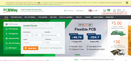
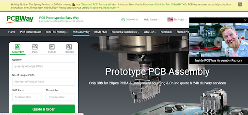
The best thing is that they provide the fastest services, and ordering online is easy here. Go to PCBWay.com and click on the PCB instant quote. They will ask for different parameters that you have to fill according to your circuit. Choose the build time and add it to the cart. You can find the detailed process on their website.
In this article, we’ll see the basic introduction of round PCBs. We’ll see the definition of round PCBs and understand how they are different from the other shapes. After that, we’ll see its manufacturing in detail and will see different phases of manufacturing. We’ll also have a look at their application. Let’s start learning.
Introduction to Round PCB
The PCBs are present in different shapes and sizes and are customized by keeping different parameters in mind such as the scope, type, and working of the circuit. Usually, people have seen rectangular or square PCBs but one must know that round PCBs bring flexibility and functionality in the design and features of the circuits. To easily understand these, let's have a look at their introduction:
"Round PCBs are different from rectangular or square PCBs in terms of shape and applications and these bring factors like space utilization in circuits and provide better performance in different scenarios."
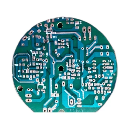
These PCBs introduce signal integrity in the high-frequency circuits because the components are tightly packed in the curved traces and as a result, better performance is gained. The difference is the presence of the curves in the round PCBs that have multiple advantages in the circuits.
Round PCBs Manufacturing
Just like other PCBs, the manufacturing of the round PCBs involves different steps and special techniques are applied in these steps. Let’s have a look at these steps:
Round PCBs Design and Garber Files
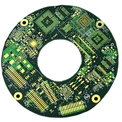
A PCB design software is used to get started with the design process of round PCBs. it creates the schematic and layout of the circuit. In the case of round PCBs, great care and attention are required because of the curves. The route tracing and component placement are different from the rectangular or square PCBs.
Once the round PCBs are designed, the process of Gerber file generation is carried out. This file has multiple instructions and information regarding the design and some of them are listed below:
- Copper layers
- Solder mask
- Silkscreen
- Drill holes
Round PCB Panel Preparation
The Garber file just discussed is used for the creation process of the photomasks. These are the essential photographic films that have patterns related to the different layers in the round PCBs. A large sheet of laminated material such as the FR4 is cut into the designed panel. A feature of this panel is, that it is pre-drilled with the registration hole so that it may be aligned with the design.
Round PCB Inner Layer Imaging and Etching
A photosensitive film (photoresist) is put to the copper foil in the laminate panel's inner layers.
The photomasks for these layers expose the required patterns to ultraviolet (UV) light. The exposed photoresist hardens, leaving the unexposed portions soft. The panel is then processed, eliminating any unexposed photoresist. This leaves the copper traces exposed. The visible copper is chemically etched away, leaving the inner layers with the appropriate circuit designs.
Round PCB’s Lamination and Drilling
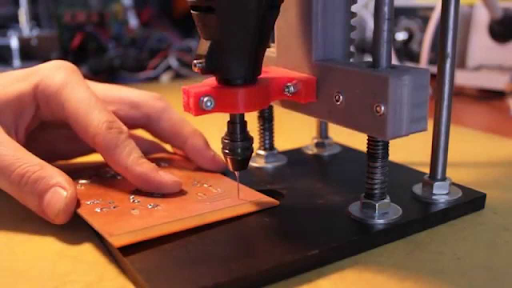
The design is now get ready with different processes such as the lamination of the surface and then drilling the holes according to the design. If the design consists of different panels then all of these are aligned together to get the best output. Once the panel is ready, the imaging and etching of the outer layer are carried out to create the final product in terms of design.
Platting of the Round PCBs
The PCBs are then passed through the process of platting. Here, a thin layer of the conducting material is applied to the required arrears to provide conductivity. Usually, this layer is copper because of its best-conducting characteristics.
Round PCB’s Soldermask and Silkscreening Process
Once the copper (or any other material) is traced on the round PCBs, a solder mask is applied to the PCB so that the traces may be protected against oxidation. In the end, the silkscreen is applied to the PCBs to add more details.
Applications of Round PCBs
The applications of the round PCBs are the same as the traditional ones but they play a crucial role in improving factors such as performance and space constraints. Here are some advantages that you must know:
Round PCBs Consumer Electronics
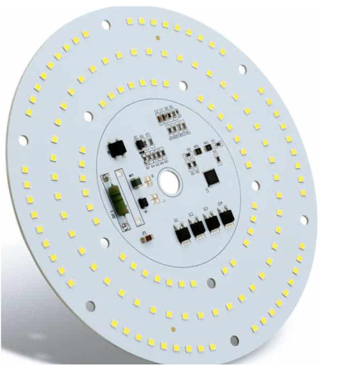
The consumer electrics are changing day by day. Smart technologies have made these electronics smaller and more stylish. The round PCBs help to get better performance in the smaller space. For instance, these are used in smartwatches, fitness trackers, and related wearables where the round shape fits into the device easily.
Round PCBs in the Medical Devices
The medical devices are becoming smaller and smarter. For instance, the large X-ray machines, or blood pressure measuring devices are smaller now and are used as wearables. The round PCBs are used here because of their round curves and smart shape to fit in these devices.
Round PCBs in the Automotive Industry
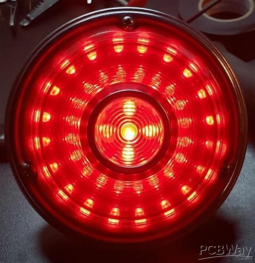
The round PCBs are not only smart but are more appealing in their looks. The automotive industry requires circuits that not only provide better performance but also look more stylish. Some automotive instrument clusters and control panels always prefer round PCBs because of their look.
As a result, we have understood the round PCBs in detail in this article. We started with the introduction to the round PCBs and then saw how these PCBs are designed and ready to work. We saw why these are better in performance and in the end, we discussed how to get the best PCBs from PCBWay.com. I hope all the points are clear now and if you want to know more, you can contact us.


