What is Laser Direct Imaging (LDI)? Role in PCB Fabrication
Hey readers! Hopefully, you are having a great day. Today, we will discuss Laser Direct Imaging (LDI) and its role in PCB fabrication. Laser Direct Imaging (LDI) is a computer-directed method that employs laser beams to expose circuit patterns directly onto photoresist-coated PCBs, without the need for conventional photomasks.
Printed Circuit Boards are the unobtrusive facilitators of contemporary technology, energizing anything from consumer products to aerospace technologies. As the pace of technology advances, however, the electronics within must make their circuits tighter, more advanced, and more efficient. Complying with these demands depends on innovation along every production process, particularly with how circuitry patterns are replicated onto the board.
This important step, imaging, formerly used photomasks and ultraviolet light to pattern-expose a photosensitive surface. Effective enough for ordinary layouts, the technique has trouble keeping pace with the growing requirement for fine-line resolution and variable production.
Laser Direct Imaging, or LDI, provides a compelling solution. Rather than employing physical masks, LDI employs digitally guided laser beams to directly expose the circuit pattern onto the photoresist layer. This maskless process allows for higher accuracy, accommodates fast design changes, and facilitates the creation of finer features with less variation.
Here, we will discover Laser Direct Imaging (LDI), its working, its role in PCB fabrications, and its advantages in detail. Let’s dive.
Where do you get LDI Services?
If you need solid and advanced LDI services, PCBWay Fabrication House has one of the industry's best solutions. With the latest Laser Direct Imaging technology and a trained production team, PCBWay provides high-resolution PCBs with outstanding trace detail, close spacing, and impeccable alignment between layers. Their technology guarantees every board is of the highest performance and precision standards.
What makes PCBWay unique is that they can mesh high-end technology with accessibility. Whether you are developing a prototype, custom design, or large-volume production job, their LDI-capable process facilitates rapid turnaround and design flexibility without compromise. It is the perfect service for engineers, startups, and tech firms who require trustworthy, fine-line PCB manufacturing. For further details, you can visit their website.
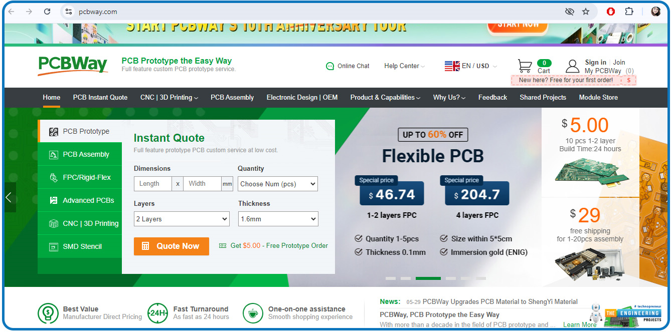
Beyond just manufacturing, PCBWay offers a smooth, user-friendly experience. From instant online quotes to expert support and fast worldwide shipping, they make it easy to bring your ideas to life. With PCBWay, you’re not just getting LDI services—you’re getting a trusted partner in innovation.
What is Laser Direct Imaging (LDI)?
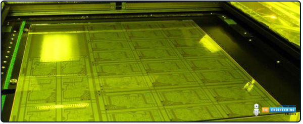
The Laser Direct Imaging approach (LDI) is a digital imaging approach at the forefront of innovation that puts patterns of circuits on photoresist-coated PCBs directly through the services of a focused beam laser. LDI does not make use of the physical photomasks or films used traditionally by photolithography since the design data projects straight from a digital file onto the PCB. This gives higher-resolution patterning with improved precision regardless of constraints in mask alignment, as shown in the figure.
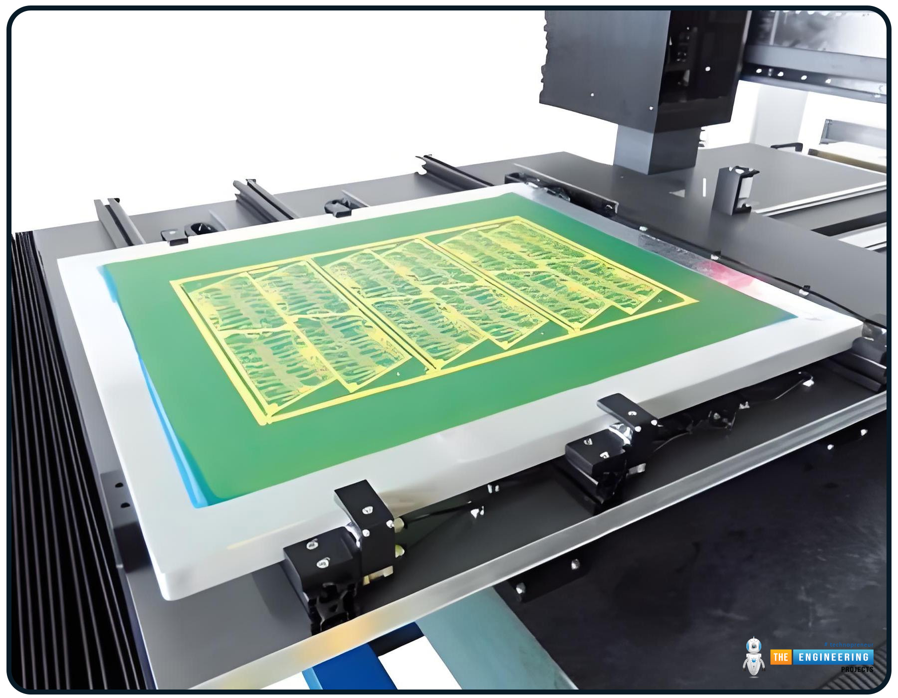
LDI also has several advantages over traditional methods of PCB fabrication. It can offer very thin trace widths and intimate spacings and thus is an excellent choice for high-density interconnect (HDI) boards and complex multi-layer PCBs. LDI is also able to support greater speed of adjustments and changes to the design, and that places it perfectly for rapid prototyping and dynamic designs. LDI by avoiding the requirement of photomasks also saves time and cost in production, offering producers a speedy and low-cost way of producing up-to-date electronic devices.
How LDI Works?
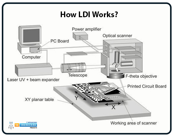
A recent process used for Printed Circuit Board ( PCB ) manufacturing, Laser Direct Imaging ( LDI ) utilizes laser technology to directly image its circuitry onto a copper clad substrate. The process has many benefits over traditional photolithography: improved accuracy, reduced processing time, and no photomask required.
1. Data Preparation:
The LDI process starts with data preparation, where the design files of the PCB, usually in Gerber or ODB++ formats, are transformed to a readable format for the LDI machine. The design files have precise information regarding the layout of the PCB, such as trace position, via position, pad position, and so on. The design is then processed by the computer inside the LDI machine to create laser instructions. This is to ensure that the laser will be able to precisely duplicate the circuit pattern on the photoresist-coated board.
2. Board Preparation:
After preparation of the data, the second step is preparation of the board. A copper-clad laminate (a sheet of copper bonded to a substrate, typically fiberglass) is coated with a layer of photo-resist, a light-sensitive material. Photoresist is a dry film or liquid photoimageable resist (LPI). Dry film resist is a solid thin film deposited, while LPI resist is deposited as a liquid and cross-linked. The layer of photoresist acts as a mask, preventing the underlying copper from being etched during the latter etching process.
3. Laser Imaging:
In the process of laser imaging, the LDI machine exposes the photoresist to light selectively using computer-controlled UV (ultraviolet) lasers. The laser inscribes the board based on the information in the PCB design file, tracing the pattern of the circuit exactly. The UV lasers reveal the photoresist in specific areas, which creates a pattern matching the traces, pads, and vias. The laser system can function with multiple beams from different angles to be able to simplify the process considerably and speed it up if the number of PCBs is high.
The accuracy of the LDI system allows it to create dense, detailed patterns with far greater accuracy for use in more subtle applications such as high-density interconnects (HDI) and microvias, where standard methods may not be able to provide the level of detail.
4. Development:
After the board has been processed using the laser, it will be developed. Developing is the process of removing the unexposed or exposed regions of the photoresist, respectively, based on whether positive or negative resist has been utilized. For positive resist, the laser-exposed area dissolves and is washed away, and the unexposed area remains to act as a pattern for traces in the PCB. In negative resist, the exposed regions become hardened, and the unexposed regions dissolve.
The board has a patterned photoresist layer after development, which is used as a mask in the next process of copper etching, where unprotected copper is removed to create the electrical traces.
Laser Direct Imaging (LDI) in PCB Fabrication:
Laser Direct Imaging (LDI) is a cutting-edge technology used in the manufacture of Printed Circuit Boards (PCBs) with increased precision, increased speed, and increased design freedom. Using computer-controlled lasers to directly print circuit patterns on a PCB, LDI has become an indispensable tool at several stages of PCB manufacturing, usually enhancing the quality and efficiency of the manufacturing process.
1. Inner Layer Imaging:
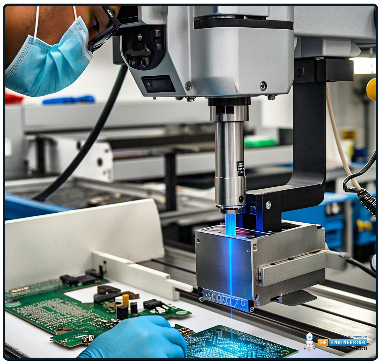
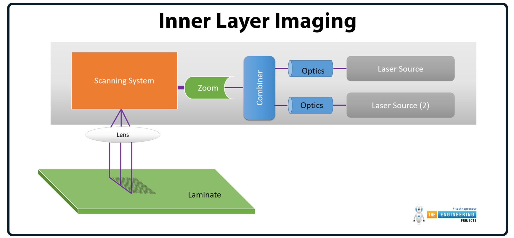
Inner layer imaging is an essential step in multilayer PCB production for the proper transfer of copper pattern onto inner layers. Patterns need to be aligned during one-on-top assembly during lamination. LDI improves positioning precision, which reduces registration error responsible for faults or malfunctions. The LDI direct writing of the photoresist prevents degradation of the inner layers since they are printed with high precision, maintaining the integrity of the design in the multilayer PCB process.
2. Outer Layer Patterning:
In outer layer patterning, LDI offers greater resolution than traditional photomasks and is essential in creating fine-pitch traces and complex component footprints. The outer layers typically contain the large circuit traces, pads, and component leads, which have to be precise, particularly with the size of PCBs decreasing and getting denser. The ability to resolve high resolution in LDI allows traces such as those for Ball Grid Array (BGA) footprints to be produced in smaller sizes and higher complexities. A similarly high degree of detail is needed for high-speed and high-frequency applications to maintain stable operation.
3. Solder Mask Imaging:
LDI also plays an important role in solder mask imaging, where the image solder mask is made over the conductive traces of the PCB and on the pads and vias on the PCB, with holes for soldering to occur. The accuracy of LDI guarantees that these holes are made to the right size and position, thereby reducing the chances of soldering failures such as bridges or open joints. The ability to form good solder mask patterns improves end PCB performance and reliability in general by preventing difficulties during assembly.
4. Photomask Removal:
One of the major advantages of LDI is the elimination of traditional photomasks. Photomasks are costly and labor-intensive to produce, creating extra steps in the PCB manufacturing process. These are eliminated with LDI, design being deposited directly onto the board, reducing cost and time to produce. This also results in turnaround time savings, making intricate PCB designs faster in delivery.
5. Greater Design Flexibility:
LDI enhances the design freedom, especially for HDI and microvia designs. LDI makes it possible for the producers to create small and intricate patterns, which suit modern high-performance devices that require miniaturized components. With an LDI, it is possible to have sophisticated designs and high-density utilisation, which leads to innovation in the manufacture of the PCBs.
Advantages of Laser Direct Imaging (LDI):
Laser Direct Imaging (LDI) has completely revolutionized the PCB manufacturing industry due to so many advantages over traditional photolithography technology. Without such technology being more accurate, more efficient, and more flexible, among other merits, no PCB manufacturing firm can produce high-performance, high-density boards.
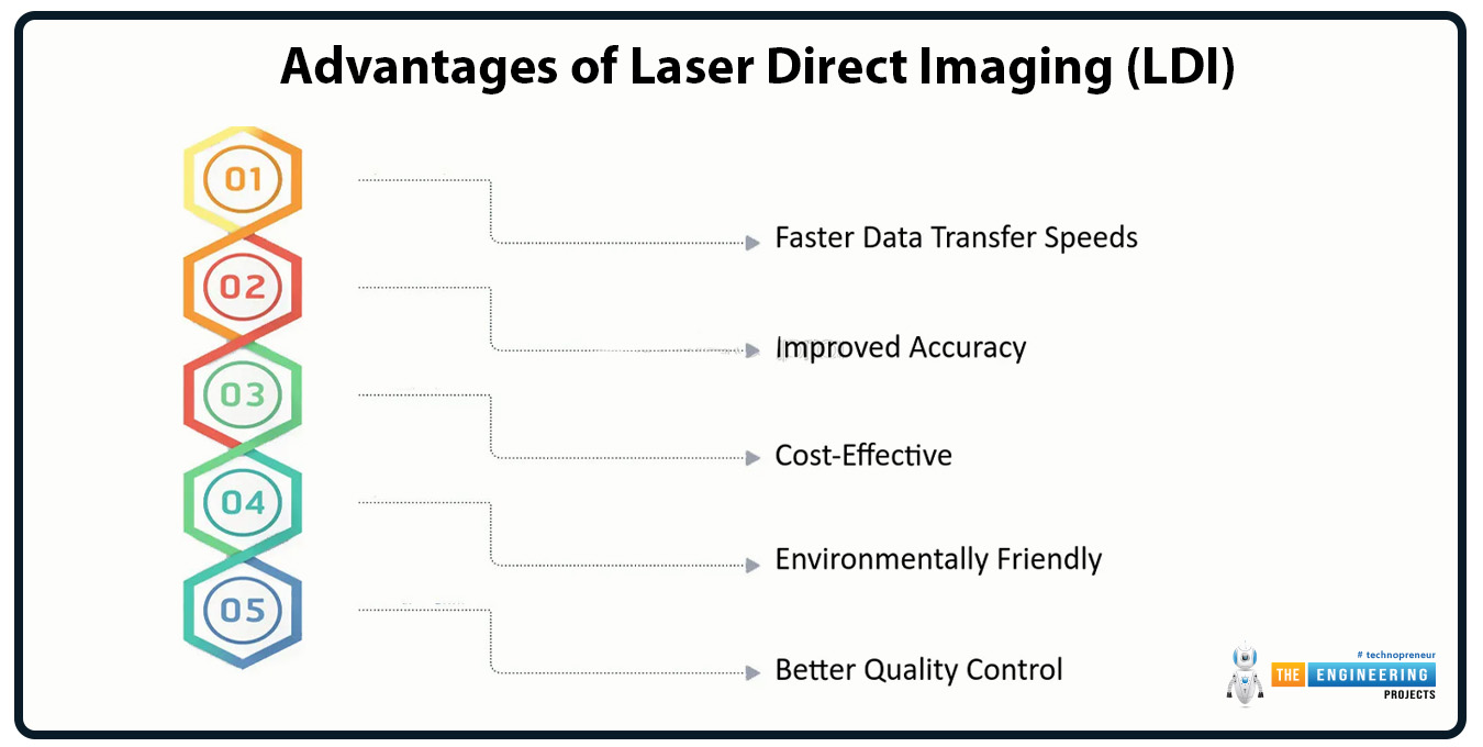
1. No Phototools Needed:
One of the largest advantages of LDI is that it eliminates phototools (photomasks). Phototools need to be created for each design in traditional PCB manufacturing, which is extremely time-consuming and expensive. LDI bypasses the requirement for physical masks by having a laser write the circuit pattern onto the photoresist directly. For quick-turn prototyping or having multiple design changes, this equates to reduced setup times, less inventory, and easier design changes.
2. High Resolution and Accuracy:
LDI provides excellent resolution, enabling the imaging of line widths and spaces of 25 microns (1 mil) or smaller. It is hard to do using conventional photolithography. As such, LDI is the ideal choice for fine line and high density PCB designs, including smartphones, medical devices, and other electronics that have shrunk in size. Its precision supports the current trend of miniaturization in electronics.
3. Improved Registration and Alignment:
With computer-aided positioning and superior optics, LDI systems enable improved registration and alignment. They utilize fiducial marks on the board to achieve precise layer-to-layer registration, a necessity in HDI and multilayer PCBs. Automatic adjustment of this sort reduces misregistration and enhances the reliability and performance of complex PCB assemblies.
4. Reduced Process Variability:
Traditional imaging methods suffer from variability caused by contamination by dust, degradation of phototools, and uneven exposure conditions. LDI avoids these by eliminating physical masks and ensuring a clean, consistent imaging process. This reduction in variability means fewer defects, higher yields, and better overall product quality.
5. Flexibility and Quick Turnaround:
LDI presents unmatched flexibility to produce. Due to the lack of photomasks, the design can be altered without delay. Hence, LDI is an excellent choice for speedy prototyping as well as production in small amounts, where speed-to-market stands as the predominant concern.
6. Lowered Environmental Impact:
LDI promotes cleaner manufacturing through the reduction of material losses associated with phototool production and film consumption. It also reduces chemical usage in development due to its cleaner, more precise imaging process. This assists in lessening the environmental footprint and conforms to modern sustainability goals in manufacturing.
Conclusion:
It is hard to do using conventional photolithography. As such, LDI is the ideal choice for fine line and high density PCB designs, including smartphones, medical devices, and other electronics that have shrunk in size. Its digital processing does away with phototools, shortening setup time and allowing for speedy design modifications—an asset in a current high-tech electronic manufacturing environment. This is perfectly suited to support rapid prototyping and low-to-moderate volume production involving high-mix.
LDI also provides higher resolution and alignment precision, critical to generating fine-line traces and multilayer PCBs with close tolerances. Through minimizing typical defects and process variability, it enhances product quality in general and increases yield. This equates to reduced manufacturing costs and more consistent end products.
Aside from its technical benefits, LDI helps ensure eco-friendly production. It avoids material wastage and chemicals, which means a minimal environmental impact. With improved technologies, LDI is not just an effective tool, but it is at present an important tool for manufacturers who want to maintain a competitive edge and future-proof.


