Reflow Soldering vs. Wave Soldering: What’s best for PCB Assembly
Hi, tech folks! Hope you're having a good day and reading about something fun and informative. Beneath every stylish device is a hard decision between wave soldering and reflow. Today, we will discuss it in detail.
In the rapidly developing electronics manufacturing universe, choosing between soldering approaches is the turning point for deciding the reliability, efficiency, and cost-effectiveness of printed circuit board (PCB) assembly. As parts continue to miniaturize, complexity increases, and there are requirements for ever-smaller miniaturized yet high-performance components, the designer must carefully choose the most effective soldering method. Among existing processes, the two universally popular processes widely employed, specific to specific processes and design applications, are reflow soldering and wave soldering.
Reflow soldering is most directly associated with Surface Mount Technology (SMT) and is noted for its precision and finesse with fine-pitch devices. Conversely, wave soldering is most typically used for through-hole technology (THT) and bulk soldering operations in simpler assemblies. While both processes are essentially aimed at achieving electric and mechanical contacts, they differ concerning the sequence of operation, equipment, material requirements, and suitability to some PCB designs.
This article discusses the basic principles, advantages, disadvantages, and general applications of both soldering methods. It also provides in-depth comparisons, process tips, and advice on selecting the best method for various PCB assembly uses. Whether you're designing consumer goods, industrial equipment, or mixed-technology boards, you need to understand these two soldering methods to guarantee manufacturing success.
Let’s dive into in-depth details.
Where can you order PCBs online?
To bring your PCB design into a good-quality manufactured board, PCBWay Fabrication House is one of the choices that are on everyone's lips for hobbyists, product developers, and experts worldwide. With their high-precision manufacturing, quick turnaround time, and decent customer service, PCBWay provides end-to-end PCB solutions, from modest beginnings of prototyping boards to intricate, production-level constructs. Anything from humble single-layer and double-layer boards to sophisticated multilayer, flex, and high-density interconnect (HDI) constructions is on the menu.
One of the best strengths of PCBWay is its capability of fabricating multilayered PCBs, which are required for today's electronics, which require miniaturized design, high-quality signals, and electromagnetic compatibility. Multilayered boards are a requirement in telecommunications, medical electronics, and embedded systems. Through the latest fabrication technologies such as controlled impedance, fine-pitch via drilling, and advanced inspection equipment, PCBWay provides stable multilayer boards responding to the high-performance requirements of today's technology. For more details, you can visit their site mentioned below.
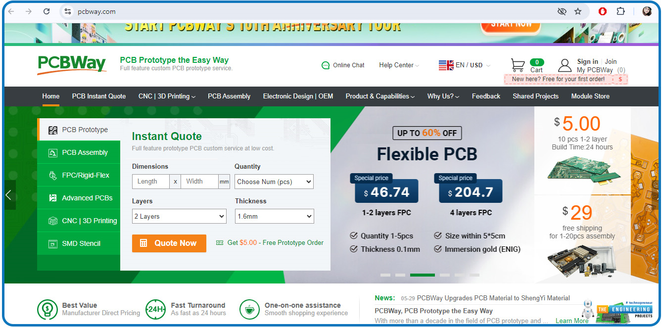
It's easy and intuitive to order. Once you're on their home page, press the "Instant Quote" button and upload your Gerber files. You'll be prompted through a step-by-step form where you can set up your board specs—num layers, materials, surface finish, copper thickness, etc. You can also include services such as PCB assembly or stencil preparation. Once submitted, your design is checked, approved, and rapidly moved into production, with status updates along the way.
Process Comparison:
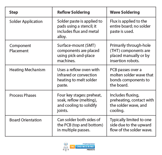
Step |
Reflow Soldering |
Wave Soldering |
Solder Application |
Solder paste is applied to pads using a stencil; it includes flux and metal alloy. |
Flux is applied to the entire board; no solder paste is used. |
Component Placement |
Surface-mount (SMT) components are placed using pick-and-place machines. |
Primarily through-hole (THT) components are placed manually or by insertion robots. |
Heating Mechanism |
Uses a reflow oven with infrared or convection heating to melt solder paste. |
PCB passes over a molten solder wave that bonds components to the board. |
Process Phases |
Four key stages: preheat, soak, reflow (melting), and cooling to solidify joints. |
Includes fluxing, preheating, contact with the solder wave, and cooling. |
Board Orientation |
Can solder both sides of the PCB (top and bottom) in multiple passes. |
Typically limited to one side due to the upward flow of the solder wave. |
In-Depth Reflow Soldering Process:
Reflow soldering is the most common assembly process of contemporary surface-mount technology (SMT) printed circuit boards (PCBs). Its accuracy, reproducibility, and amenability to miniaturized devices make it highly suitable for high-density and high-performance electronics.
Major Steps:
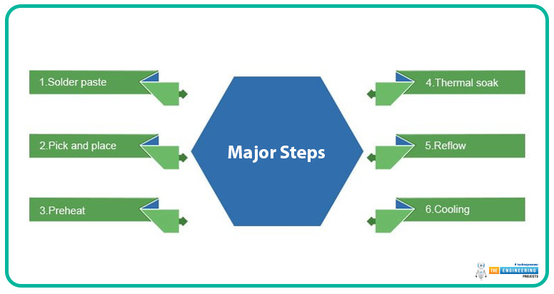
Stencil Printing: The process starts by depositing solder paste onto the PCB pads using a stainless steel stencil. The paste is a blend of fine solder particles and flux.
Component Placement: Robotic pick-and-place machines precisely position SMT components onto solder-paste-coated pads. The machines are quick, precise, and well-suited for placing fine-pitch packages such as BGAs and QFNs.
Preheat Zone: As the board goes into the reflow oven, it first passes through a preheat zone. The temperature is increased stepwise to minimize thermal shock and to start activating the flux.
Soak Zone: Board temperature is held steady in the soak zone as the flux dissolves the oxides off of component leads and pads.
Reflow Zone: The temperature is up to approximately 220°C to 250°C, soldering the melting and forming good, strong electrical and mechanical connections.
Cooling Zone: Controlled cooling of the board freezes solder joints and forms good metallurgical contacts.
Advantages:
Best for High-Density Boards: Reflow soldering performs well with densely populated boards and small or fragile components like BGAs and QFNs.
Double-Sided Feasible: The process permits the population of both sides of the PCB, usually with multiple trips through the reflow oven.
Highly Automated: With little or no hand labor, the process is repeatable and consistent, ideal for high-volume SMT production.
Accurate: Best suited to fine-pitch components where location and controlled temperature are important.
Limitations
Incompatibility with Through-Holes: Reflow does not work well with through-hole components other than for selective soldering.
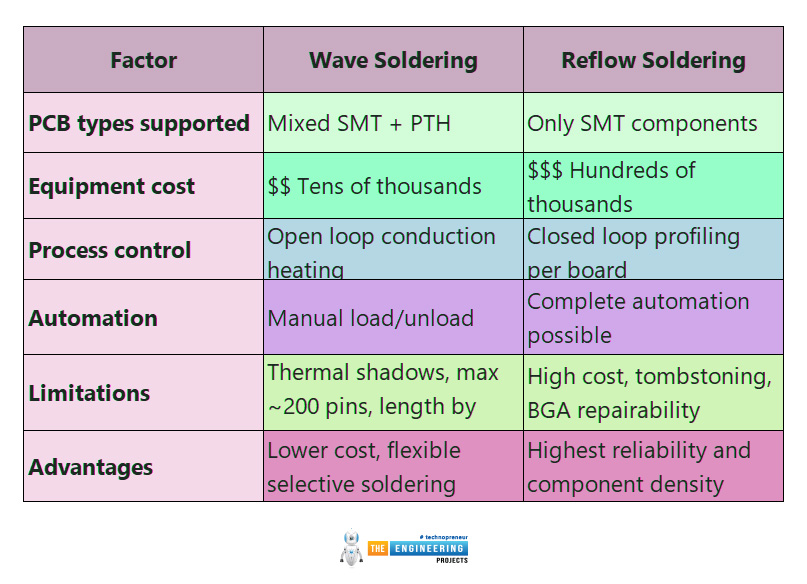
High Cost of Equipment: Reflow ovens and solder paste printers are costly, with high initial capital costs.
Solder Paste Control: Solder paste has to be stored and handled correctly with limited shelf life and temperature, as well as humidity sensitivity.
High-Tech Wave Soldering Process:
Wave soldering is still used in more conventional through-hole component assembly and appears in reduced or high-production designs. Wave soldering uses a literal "wave" of molten solder to create the joints and thereby gets its name.
Key Steps:
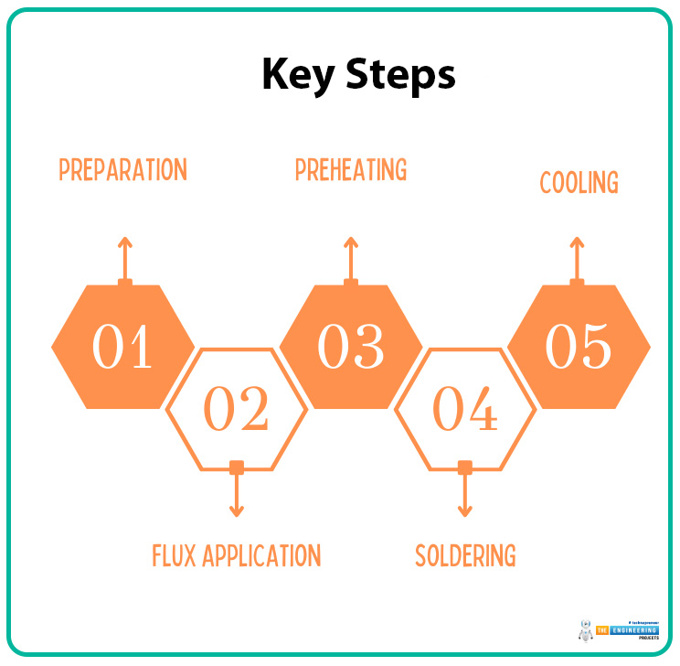
Flux Application: Solder flux is applied to the PCB bottom during soldering to suppress oxidation and enhance wetting.
Preheat Zone: The board is preheated to drive out solvent from the flux and cut back on thermal shock upon contact with the molten solder.
Solder Wave Contact: The PCB travels over a wave of flowing, liquid solder continuously, usually around 250°C. The solder contacts exposed leads and pads on the back side and forms joints in an instant.
Cooling Zone: Cools the board to set the joints and lock pieces into place.
Advantages:
Rapid for THT Assemblies: Solder a few joints in a single sweep—good for large volumes.
Setup Cost Reduced: Ideal for smaller PCB designs with no cost of solder paste or ovens.
Soldering Parallel: Wave solder enables soldering hundreds of joints simultaneously, saving production time.
Limitations:
Limited SMT Support: It accommodates not-so-densely packed SMT boards and low-pitch parts inadequately.
Defects: Solder bridging and bad wetting are typical defects in poorly designed processes.
One-Sided Soldering: Effective soldering is possible only on the back side of the PCB, and the layout becomes restrictive.
Thermal Stress: Parts can get damaged due to the sudden heat of the solder wave if preheating is incorrectly performed.
Applications and Use Cases:
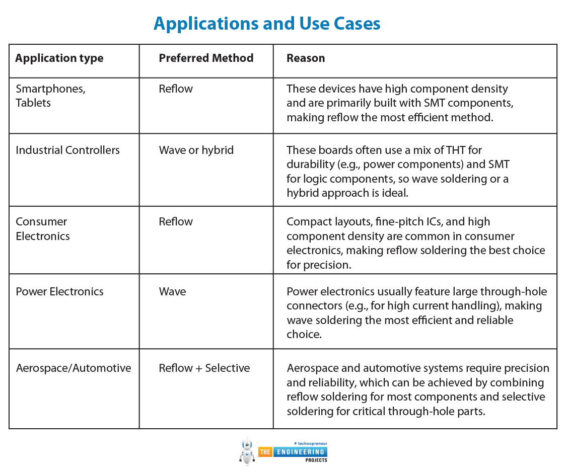
Application type |
Preferred Method |
Reason |
Smartphones, Tablets |
Reflow |
These devices have high component density and are primarily built with SMT components, making reflow the most efficient method. |
Industrial Controllers |
Wave or hybrid |
These boards often use a mix of THT for durability (e.g., power components) and SMT for logic components, so wave soldering or a hybrid approach is ideal. |
Consumer Electronics |
Reflow |
Compact layouts, fine-pitch ICs, and high component density are common in consumer electronics, making reflow soldering the best choice for precision. |
Power Electronics |
Wave |
Power electronics usually feature large through-hole connectors (e.g., for high current handling), making wave soldering the most efficient and reliable choice. |
Aerospace/Automotive |
Reflow + Selective |
Aerospace and automotive systems require precision and reliability, which can be achieved by combining reflow soldering for most components and selective soldering for critical through-hole parts. |
Double-Sided PCB Assembly:
Double-sided PCBs are becoming more common in small, high-performance electronics because they can mount components on both sides of the board.
Reflow Capability:
Perfectly suited for double-sided SMT assembly.
Usually, the heavier side is assembled first.
Flip the board and reflow the second side (lighter components) in a second pass.
First-pass solder joints are made to tolerate a second heat cycle.
The process is completely automated and effective for high-volume production.
Wave Limitations:
Gravity can make THT components on the top side drop during soldering.
SMT components on the bottom need adhesives to remain in position.
More handling and complexity can result in greater production costs.
Selective soldering is frequently utilized to address individual THT joints without impacting pre-soldered SMT components.
Less suitable for high-density or double-sided SMT boards.
Thermal Profiles and Process Control:
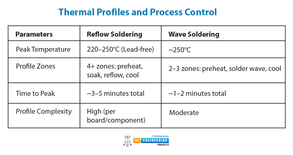
Parameters |
Reflow Soldering |
Wave Soldering |
Peak Temperature |
220–250°C (Lead-free) |
~250°C |
Profile Zones |
4+ zones: preheat, soak, reflow, cool |
2–3 zones: preheat, solder wave, cool |
Time to Peak |
~3–5 minutes total |
~1–2 minutes total |
Profile Complexity |
High (per board/component) |
Moderate |
Defect Rates and Quality Considerations:
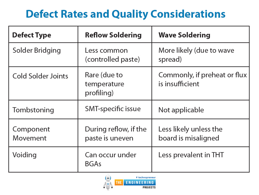
Defect Type |
Reflow Soldering |
Wave Soldering |
Solder Bridging |
Less common (controlled paste) |
More likely (due to wave spread) |
Cold Solder Joints |
Rare (due to temperature profiling) |
Commonly, if preheat or flux is insufficient |
Tombstoning |
SMT-specific issue |
Not applicable |
Component Movement |
During reflow, if the paste is uneven |
Less likely unless the board is misaligned |
Voiding |
Can occur under BGAs |
Less prevalent in THT |
Cost and Throughput Comparison:
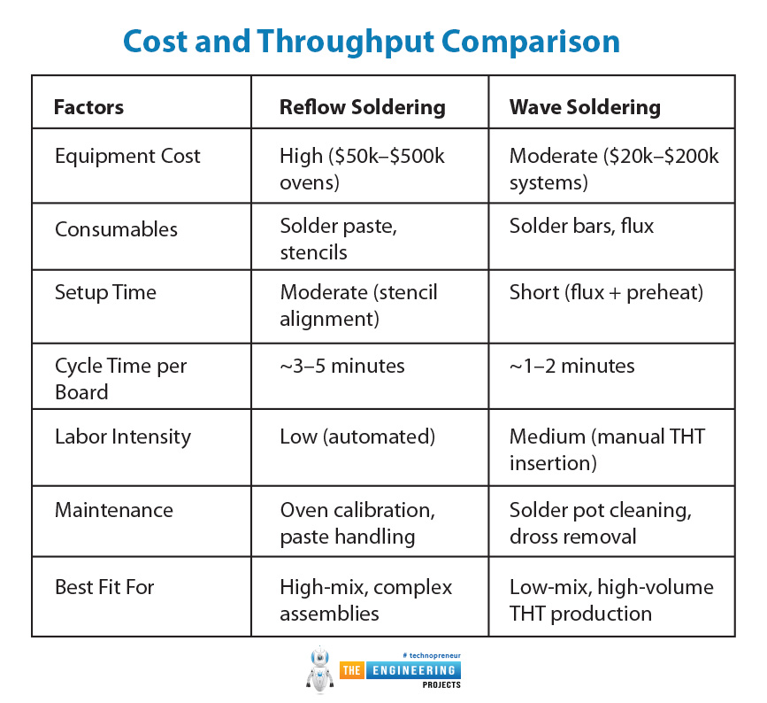
Factors |
Reflow Soldering |
Wave Soldering |
Equipment Cost |
High ($50k–$500k ovens) |
Moderate ($20k–$200k systems) |
Consumables |
Solder paste, stencils |
Solder bars, flux |
Setup Time |
Moderate (stencil alignment) |
Short (flux + preheat) |
Cycle Time per Board |
~3–5 minutes |
~1–2 minutes |
Labor Intensity |
Low (automated) |
Medium (manual THT insertion) |
Maintenance |
Oven calibration, paste handling |
Solder pot cleaning, dross removal |
Best Fit For |
High-mix, complex assemblies |
Low-mix, high-volume THT production |
Environmental and Material Implications:
Both wave and reflow soldering need to meet current environmental regulations, particularly with the transition to lead-free processes under RoHS regulations. Material and environmental implications for each are different.
Reflow Soldering:
Ideally suited for lead-free alloys, most often using the SAC305 alloy.
No-clean solder pastes lower post-process cleaning and minimize flux residues.
Some sensitive assemblies can have a nitrogen atmosphere in the reflow oven to minimize oxidation.
Less material waste than with wave soldering.
Wave Soldering:
Also suitable for lead-free alloys, but leads to increased solder dross formation.
Needs efficient fume extraction systems because of flux vapors and residues.
Board warping may happen on larger PCBs because of non-uniform heating and mechanical stress.
More solder and flux are generally used per board, with greater material handling requirements.
Choosing the Right Method: Summary Guide
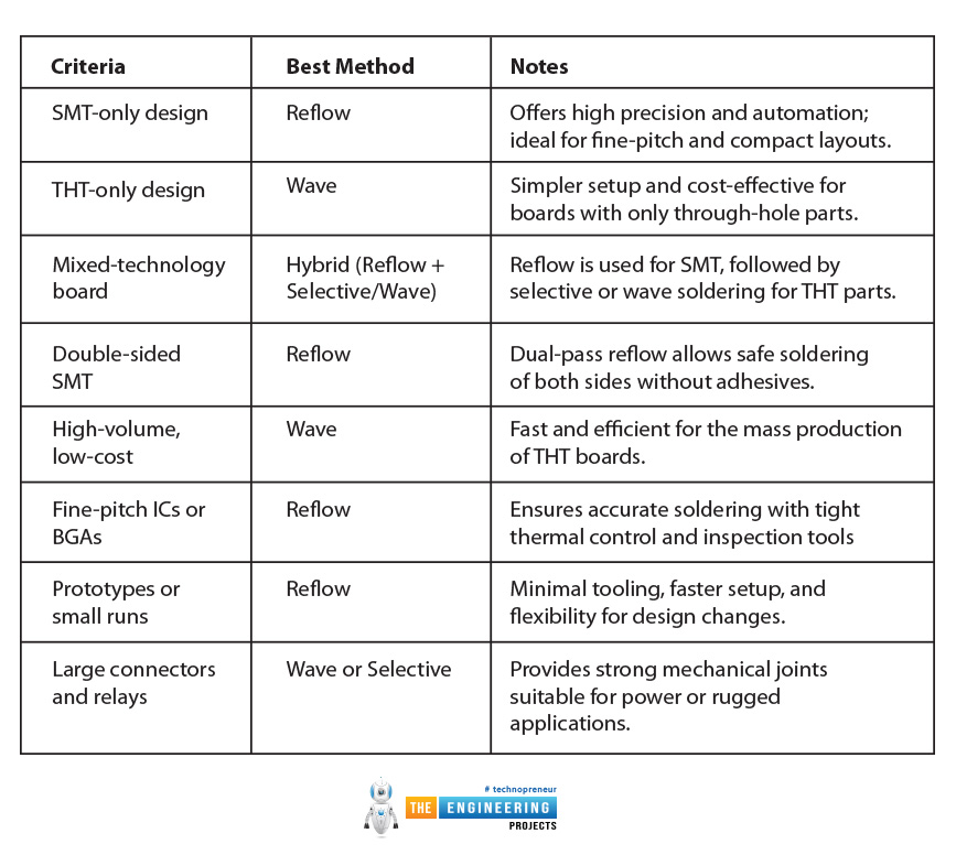
Criteria |
Best Method |
Notes |
SMT-only design |
Reflow |
Offers high precision and automation; ideal for fine-pitch and compact layouts. |
THT-only design |
Wave |
Simpler setup and cost-effective for boards with only through-hole parts. |
Mixed-technology board |
Hybrid (Reflow + Selective/Wave) |
Reflow is used for SMT, followed by selective or wave soldering for THT parts. |
Double-sided SMT |
Reflow |
Dual-pass reflow allows safe soldering of both sides without adhesives. |
High-volume, low-cost |
Wave |
Fast and efficient for the mass production of THT boards. |
Fine-pitch ICs or BGAs |
Reflow |
Ensures accurate soldering with tight thermal control and inspection tools |
Prototypes or small runs |
Reflow |
Minimal tooling, faster setup, and flexibility for design changes. |
Large connectors and relays |
Wave or Selective |
Provides strong mechanical joints suitable for power or rugged applications. |
Conclusion:
Reflow and wave soldering are both essential to contemporary PCB assembly, each with particular design and production applications. Reflow soldering is the method of choice for SMT designs, with high accuracy, automation, and support of compact, double-sided board arrangements. It is especially good at assembling fine-pitch devices and intricate circuitry that is typical of today's electronics.
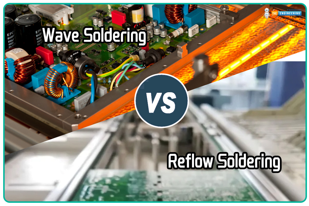
Whereas wave soldering is still worthwhile for through-hole components and volume production of easier boards, it offers robust mechanical joints and cost-effective soldering of numerous leads in a single pass, thereby being well suited to connectors and big parts.
As things become more sophisticated, hybrid methodologies that blend reflow with wave or selective soldering are progressively prevalent. The approach is designed to balance price, reliability, and flexibility.
Knowing when and how to use each of these techniques is most important in minimizing defects, maximizing production, and speeding product development. Instead of one being better than the other, the best strategy is to pick the appropriate method for every assembly challenge.


